Wired circuit board and production method thereof

a technology of wired circuit boards and production methods, applied in the direction of sustainable manufacturing/processing, coupling device connections, final product manufacturing, etc., can solve the problems of resin film, the actual position of the opening formed may be displaced, so as to reduce costs and high productivity

Active Publication Date: 2008-08-05
NITTO DENKO CORP
View PDF5 Cites 5 Cited by
  • Summary
  • Abstract
  • Description
  • Claims
  • Application Information

AI Technical Summary

Benefits of technology

[0015]It is an object of the present invention to provide a wired circuit board that can realize cost reduction by determining defectiveness in a simple and reliable manner, while ensuring high productivity, and a production method of the same.
[0017]In the wired circuit board of the present invention, the position determining zone for determining whether or not the margin of the insulating cover layer facing the opening is located in a proper position is provided in proximity of the terminal portions. This can allow easy determination whether or not the margin of the insulating cover layer is located in a proper position by reference to the position determining zone and thus can allow easy determination whether or not the actual position of the opening of the insulating cover layer formed is displaced from the designed position of the opening. By virtue of this, a wired circuit board can be provided that can realize cost reduction by determining defectiveness of the wired circuit board in a reliable and simple manner, while ensuring high productivity.
[0022]In the production method of the wired circuit board of the present invention, when the margin of the insulating cover layer is situated in the position determining zone, the wired circuit board is determined as non-defective, while on the other hand, when the margin of the insulating cover layer is not situated in the position determining zone, the wired circuit board is determined as defective. This configuration can provide easy determination whether or not the actual position of the opening of the insulating cover layer is displaced from the designed position of the opening by reference to the position determining zone, and, whereby easy determination can be made on the defective / non-defective of the wired circuit board. As a result, this can provide a wired circuit board that can realize cost reduction by determining defectiveness of the wired circuit in a reliable and simple manner, while ensuring high productivity.

Problems solved by technology

However, any of the first to third methods outlined above has a possible problem that an actual position of the opening formed may be displaced from a designed position of the opening.
Specifically, the first method has a possible problem that due to possible displacement of the photo mask in the photo process, the actual position of the opening formed may be displaced from the designed position of the opening.
The second method has a possible problem that due to possible pattern misalignment that may be caused by displacement of the solder resist in the printing process, the actual position of the opening formed may be displaced from the designed position of the opening, or an actual dimension of the opening formed is deviated from the designed dimension of the opening.
Further, the third method involves possible problems that the insulating resin film having the opening previously formed may be adhesively bonded with the opening displaced from the designed position, that the insulating resin film may be bored after bonding at a position displaced from the designed position of the opening of the insulating resin film, and that the opening may be bored with its actual dimension deviated from the designed dimension of the opening.
If the actual position of the opening formed is displaced from the designed position of the opening, then the terminal portions are covered with the insulating cover layer, in other words, is exposed so insufficiently that an electronic component cannot be mounted, so that it causes difficulties in mounting the electronic component reliably.
However, this known measuring method takes a lot of troubles with the determination of the displacement, and thus have difficulties in realizing cost reduction while ensuring high productivity.

Method used


Image

  • Wired circuit board and production method thereof
  • Wired circuit board and production method thereof
  • Wired circuit board and production method thereof

Examples


Embodiment Construction

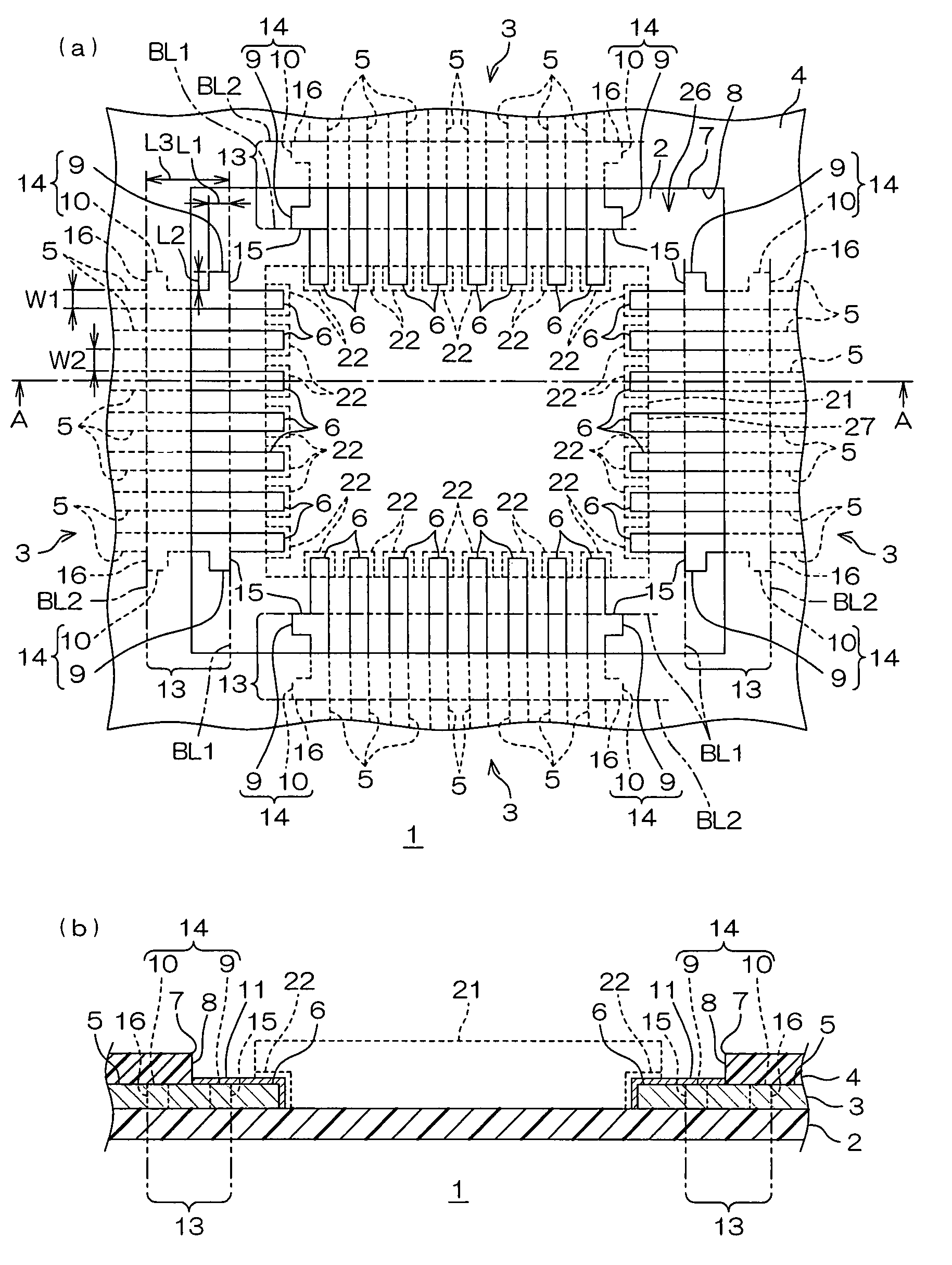
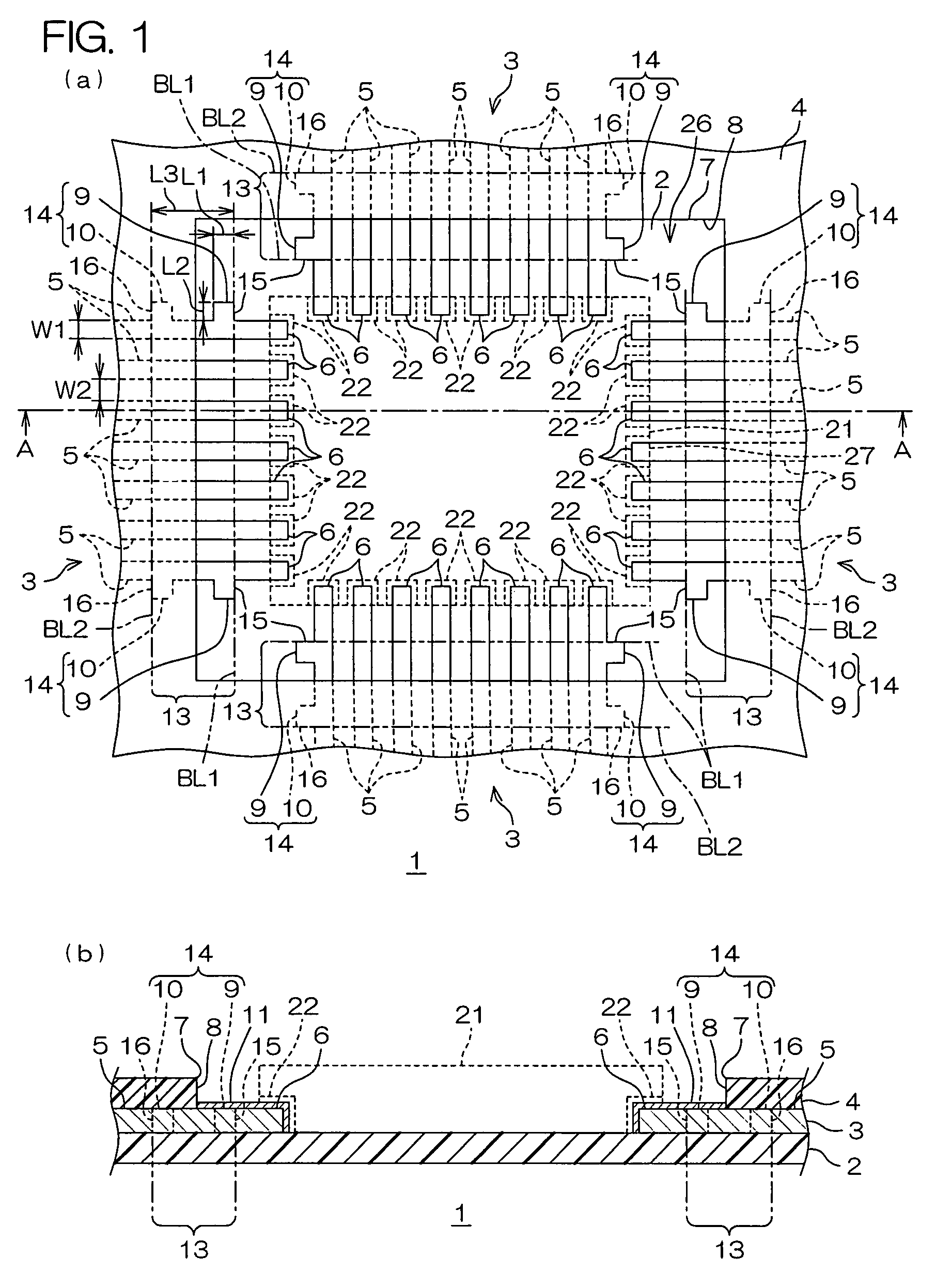
[0043]FIG. 1(a) is an enlarged plan view showing a mounting area of a wired circuit board of an embodiment of the present invention. FIG. 1(b) is an enlarged sectional view of the mounting area of the wired circuit board taken along line A-A shown in FIG. 1(a).

[0044]The wired circuit board 1 is, for example, a flexible wired circuit board extending in a generally rectangular strip form, as viewed from top, though not shown. This wired circuit board 1 includes, at both end portion thereof, a mounting area 26 shown in FIG. 1(a). A mounting portion 27 in a generally rectangular form, as viewed from top, for mounting an electronic component 21 is provided in each the mounting area 26.

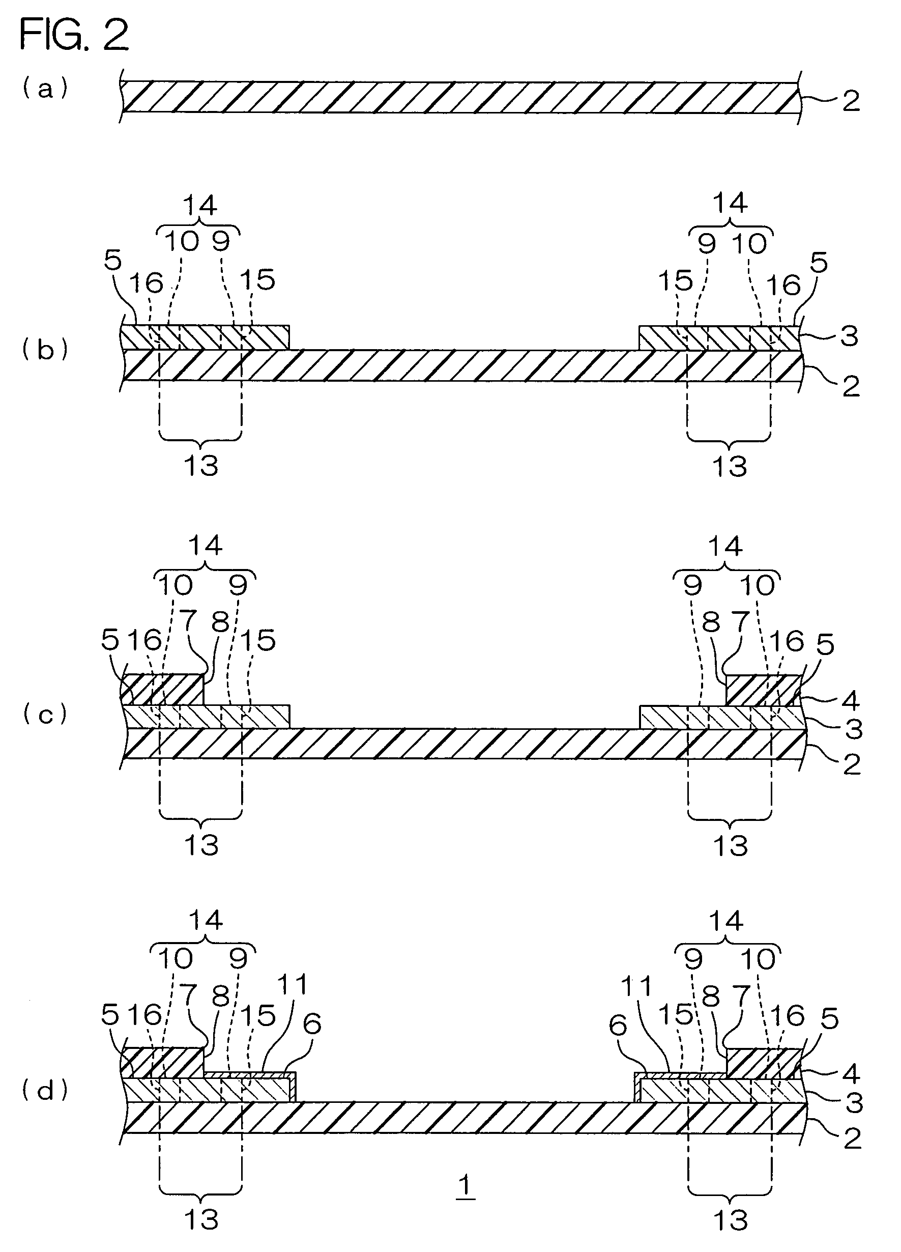
[0045]Further, the wired circuit board 1 includes an insulating base layer 2, a conductive pattern 3 formed on the insulating base layer 2, and an insulating cover layer 4 formed on the insulating base layer 2 for covering the conductive pattern 3, as shown in FIG. 1(b).

[0046]The insulating base layer 2 is ...


PUM


Abstract

A wired circuit board includes an insulating base layer, a conductive pattern formed on the insulating base layer, and an insulating cover layer formed on the insulating base layer for covering the conductive pattern. The conductive pattern includes terminal portions for connecting with external terminals. The insulating cover layer has an opening formed correspondingly for the respective terminal portions. A position determining zone for determining whether or not a margin of the insulating cover layer facing the opening is located in a proper position is provided in proximity of the terminal portions.

Description

CROSS REFERENCE TO RELATED APPLICATION[0001]This application is an application claiming priority based on Japanese Patent Application No. 2006-36727 filed on Feb. 14, 2006, the disclosure of which is incorporated herein by reference.BACKGROUND OF THE INVENTION[0002]1. Field of the Invention[0003]The present invention relates to a wired circuit board and to a production method thereof. More particularly, the present invention relates to a wired circuit board having terminals connected to external terminals and to a production method of the same.[0004]2. Description of the Prior Art[0005]The wired circuit board commonly comprises a conductive pattern comprising a plurality of wires formed on an insulating base layer, and an insulating cover layer formed on the insulating base layer for covering the conductive pattern.[0006]In this wired circuit board, the conductive pattern has terminal portions for connecting to external terminals of an electronic component and the like, and the insu...

Claims


Application Information

Patent Timeline
Patent Type & Authority Patents(United States)
IPC IPC(8): H01R12/00
CPCH01L23/544H05K1/0269H05K1/111H05K3/3452H01L24/81H05K2203/166H05K2203/163H01L2223/5442H01L2223/54473H01L2223/54486H01L2224/81801H01L2924/15153H01L2924/1517H05K2201/09781H05K2201/0989H05K2201/10674H01L2224/81143H01L2924/12042H01L2924/14Y02P70/50H01L2924/00H05K1/09
Inventor ICHIKAWA, KAZUSHITAKAYOSHI, YUICHI
Owner NITTO DENKO CORP
Why Eureka
Try Eureka