Thin film transistor, thin film transistor array and repairing method thereof

a thin film transistor and array technology, applied in the field of thin film transistors, can solve problems such as non-conformity among pattern positions, and achieve the effect of poor display quality

Active Publication Date: 2008-08-05
NYTELL SOFTWARE LLC
View PDF5 Cites 4 Cited by
  • Summary
  • Abstract
  • Description
  • Claims
  • Application Information

AI Technical Summary

Benefits of technology

[0012]An object of the present invention is to provide a thin film transistor (TFT) may be used in TFT arrays to avoid nonconformity of gate-drain parasitic capacitances in each TFT caused by the exposure process error during a TFT array process.
[0013]Another object of the present invention is to provide a thin film transistor array (TFT array) to avoid the nonconformity of feed-through voltages in each pixel caused by the exposure process error during a TFT array process.
[0014]A further object of the present invention is to provide a method for repairing thin film transistor arrays (TFT arrays) to reduce the bright spots on the display.
[0025]The present invention provides a TFT having a gate with special design, which can avoid poor display quality encountered in the prior art caused by the exposure process error during TFT array process.

Problems solved by technology

Wherein, a displacement error during movements of the stepper would cause nonconformity among the pattern positions in each shot region.

Method used


Image

  • Thin film transistor, thin film transistor array and repairing method thereof
  • Thin film transistor, thin film transistor array and repairing method thereof
  • Thin film transistor, thin film transistor array and repairing method thereof

Examples


Embodiment Construction

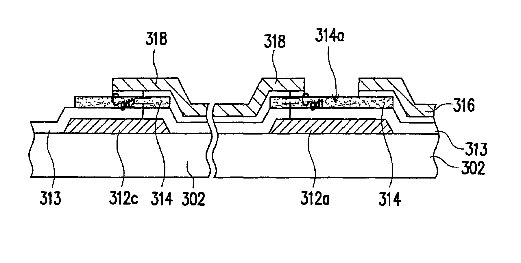
[0033]FIG. 3 is partial top view of a TFT array in the first embodiment of the present invention. FIG. 4 is a cross-sectional view along plane I-I′ of the TFT array in FIG. 3. Referring to FIG. 3, a TFT array 300 mainly includes a substrate 302, a plurality of TFTs 310 and a plurality of pixel electrodes 320. Wherein, scan lines 304 and data lines 306 are disposed on the substrate 302 and the substrate 302 is partitioned into a plurality of pixel regions by the scan lines 304 and data lines 306. One TFT 310 and one pixel electrode 320 are disposed in each of the pixel regions. The structure of the TFT 310 is described hereinafter in more details.

[0034]Referring to FIGS. 3 and 4, a TFT 310 mainly includes a gate 312, a semiconductor layer 314, a source 316 and a drain 318. The gate 312 is disposed on the substrate 302 and electrically connected to the scan line 304. In particular, the gate 312 has a control part 312a, a connection part 312b and a capacitance compensation part 312c, w...


PUM


Abstract

A thin film transistor (TFT) including a gate, a semiconductor layer, a source and a drain is provided. The gate has a control part, a connection part and a capacitance compensation part. The connection part is disposed between the control part and the capacitance compensation part for joining the two parts together. The semiconductor layer is disposed over the gate, the source and the drain are disposed on the semiconductor layer. An end of the drain overlaps the control part of the gate with a first region for composing a first parasitic capacitance; while another end of the drain overlaps the capacitance compensation part of the gate with a second region for composing a second parasitic capacitance. In a TFT array with the TFT, the sum of the first parasitic capacitance and the second parasitic capacitance is a constant.

Description

BACKGROUND OF THE INVENTION[0001]1. Field of Invention[0002]The present invention relates to a thin film transistor (TFT), and particularly to a thin film transistor (TFT), a thin film transistor array (TFT array) and a repairing method thereof capable of enhancing even brightness of a LCD panel.[0003]2. Description of the Related Art[0004]The rapid development in the multimedia industry is largely attributed to the progress in the semiconductor devices or display apparatuses. In terms of displays, the TFT liquid crystal displays (TFT-LCDs), with such advantages as high display quality, high space utilization, low power consumption and no radiation, have played a major role in the mainstream display market.[0005]A TFT-LCD mainly includes a TFT array, a color filter and a liquid crystal layer. FIG. 1 is a top view of a conventional thin film transistor array (TFT array). Referring to FIG. 1, a TFT array 100 mainly includes a plurality of pixel structures 110 arranged to form an array...

Claims


Application Information

Patent Timeline
Patent Type & Authority Patents(United States)
IPC IPC(8): H01L29/15H01L29/04
CPCH01L27/124G02F2001/13606G02F2001/13625H01L29/66757G02F2001/136268G02F1/13606G02F1/13625G02F1/136268
Inventor LIU, WEN-HSIUNG
Owner NYTELL SOFTWARE LLC
Why Eureka
Try Eureka