Switching power supply device, semiconductor integrated circuit device and power supply device

a power supply device and integrated circuit technology, applied in the direction of dc-dc conversion, oscillation generator, power conversion system, etc., can solve the problems of high-frequency operation, leakage current caused by lowering voltage tend to increase, and the design of the power supply circuit becomes very difficult in order to meet these requirements, and achieves fast response of the switching power supply device, stable operation, and easy operation

Inactive Publication Date: 2008-08-05
RENESAS ELECTRONICS CORP
View PDF6 Cites 24 Cited by
  • Summary
  • Abstract
  • Description
  • Claims
  • Application Information

AI Technical Summary

Benefits of technology

[0006]The operating frequency of a recent PC (personal computer) and a system control unit (memory, CPU, and GPU) mounted on a server is being faster year by year for increasing processing capacity. A supply voltage thereof is being lowered. Both electric current consumption increased by high-frequency operation and a leak current caused due to lowered voltage tend to increase. A power supply circuit is required to provide increased accuracy of a supply voltage, fast response for preventing lowered supply voltage at sudden change in load, and stabile operation. The design of the power supply circuit becomes very difficult in order to meet these requirements.
[0008]FIG. 12 shows a schematic block diagram of a peak current control system which has been studied prior to this invention. FIG. 13 shows an operating waveform diagram thereof. In the peak current control system, output voltage Vout and input current IL / N are monitored and there are two feedback loops FB1 and FB2. The instable element of the feedback loop system can be cancelled. The phase compensation becomes easy. The loop gain need not be dropped excessively. The switching power supply device of the peak current control system is a circuit suitable for fast load response of a power supply. High accuracy current detection is necessary for monitoring the input current. The circuit construction of the peak current control system is more complicated than that of the voltage control system. Output current IL is detected from the switch node of the power supply circuit. Unnecessary current information such as spike noise need be cancelled.
[0018]The stable operation is possible with fast response of the switching power supply device.
[0019]Plural power supply devices can be easily operated in parallel. The parallel operation can change and increase the current supply capability. Noise reduction is easy. Fast response and increased efficiency are possible.

Problems solved by technology

Both electric current consumption increased by high-frequency operation and a leak current caused due to lowered voltage tend to increase.
The design of the power supply circuit becomes very difficult in order to meet these requirements.
It is difficult to stabilize the feedback loop system.
Fast response is impossible since the loop gain need be dropped.
The circuit construction of the peak current control system is more complicated than that of the voltage control system.

Method used


Image

  • Switching power supply device, semiconductor integrated circuit device and power supply device
  • Switching power supply device, semiconductor integrated circuit device and power supply device
  • Switching power supply device, semiconductor integrated circuit device and power supply device

Examples


Embodiment Construction

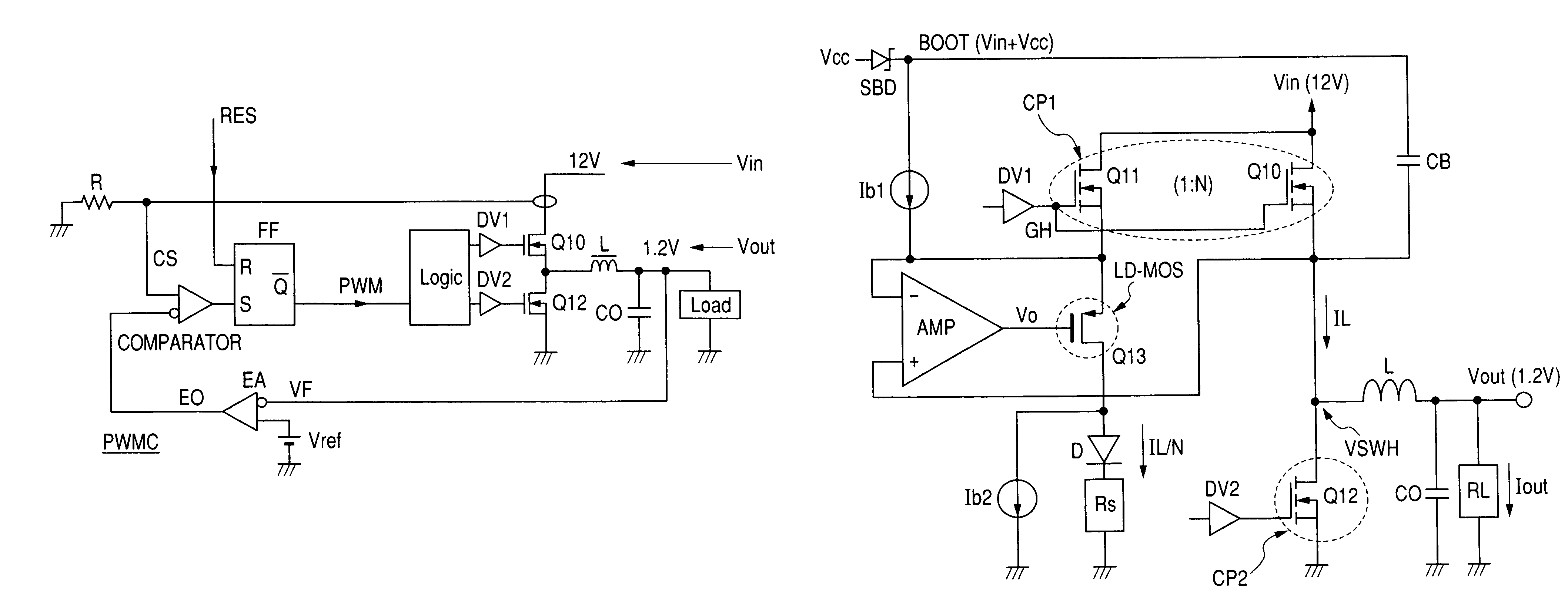
[0050]FIG. 1 shows an essential part schematic circuit diagram of an embodiment of a switching power supply device according to this invention. This embodiment is intended for a voltage drop type switching power supply device which forms output voltage Vout obtained by dropping input voltage Vin. Without being particularly limited, the input voltage Vin is a relatively high voltage of e.g., 7 to 16V, and the output voltage Vout is a low voltage of about 1.2V. The drawing shows an example in which the input voltage Vin is 12V.

[0051]The input voltage Vin supplies electric current IL from the input side of inductor L via high potential side switch MOSFETGH. Capacitor C is provided between the output side of the inductor L and circuit ground potential GND. Such capacitor C smoothens the input voltage Vin to form the output voltage Vout. The output voltage Vout is an operating voltage of load circuit RL such as a microprocessor CPU. Switch MOSFETGL is provided between the input side of t...


PUM


Abstract

There are provided a switching power supply device performing a stable operation with fast response, a semiconductor integrated circuit device, and a power supply device.A capacitor is provided between the output side of an inductor and a ground potential. A first power MOSFET supplies an electric current from an input voltage to the input side of the inductor. A second power MOSFET turned on when the first power MOSFET is off allows the input side of the inductor to be of a predetermined potential. A first feedback signal corresponding to an output voltage obtained from the output side of the inductor and a second feedback signal corresponding to an electric current flowed to the first power MOSFET are used to form a PWM signal. The first power MOSFET has plural cells of a vertical type MOS-construction. The number of cells is 1 / N. A detection MOSFET in which the gains and the drains are shared over the same semiconductor substrate with the first power MOSFET is provided to form a second feedback signal.

Description

CROSS-REFERENCE TO RELATED APPLICATION[0001]The present application claims priority from Japanese patent application No. 2006-231129 filed on Aug. 28, 2006, No. 2005-323832 filed on Nov. 8, 2005 and No. 2006-5512, filed on Jan. 13, 2006, the contents of which are hereby incorporated by reference into this application.BACKGROUND OF THE INVENTION[0002]The present invention relates to a switching power supply device, a semiconductor integrated circuit device, and a power supply device. For instance, the present invention relates to a technique effective to be applied to a switching power supply device converting a high voltage to a low voltage and a semiconductor integrated circuit device used therefor.[0003]There is U.S. Pat. No. 6,559,684 as a switching power supply device. There is “Fundamentals of Power Electronics Second Edition”, pp. 439-449, published by KLUWER ACADEMIC PUBLISHERS in the United States, as a technical document related to a switching power supply device.[0004][Pat...

Claims


Application Information

Patent Timeline
Patent Type & Authority Patents(United States)
IPC IPC(8): H03K3/00
CPCH02M3/156H03K2217/0027
Inventor NAGASAWA, TOSHIOKUDO, RYOTARO
Owner RENESAS ELECTRONICS CORP
Why Eureka
Try Eureka