

Interconnections for flip-chip using lead-free solders and having reaction barrier layers
a technology of flip-chips and solders, applied in the direction of electrical equipment, semiconductor devices, semiconductor/solid-state device details, etc., can solve the problems of limiting the extendibility of large wafers, pb-free applications, and more dense arrays
- Summary
- Abstract
- Description
- Claims
- Application Information
AI Technical Summary
Benefits of technology
Problems solved by technology
Method used
Image

Examples
example 1
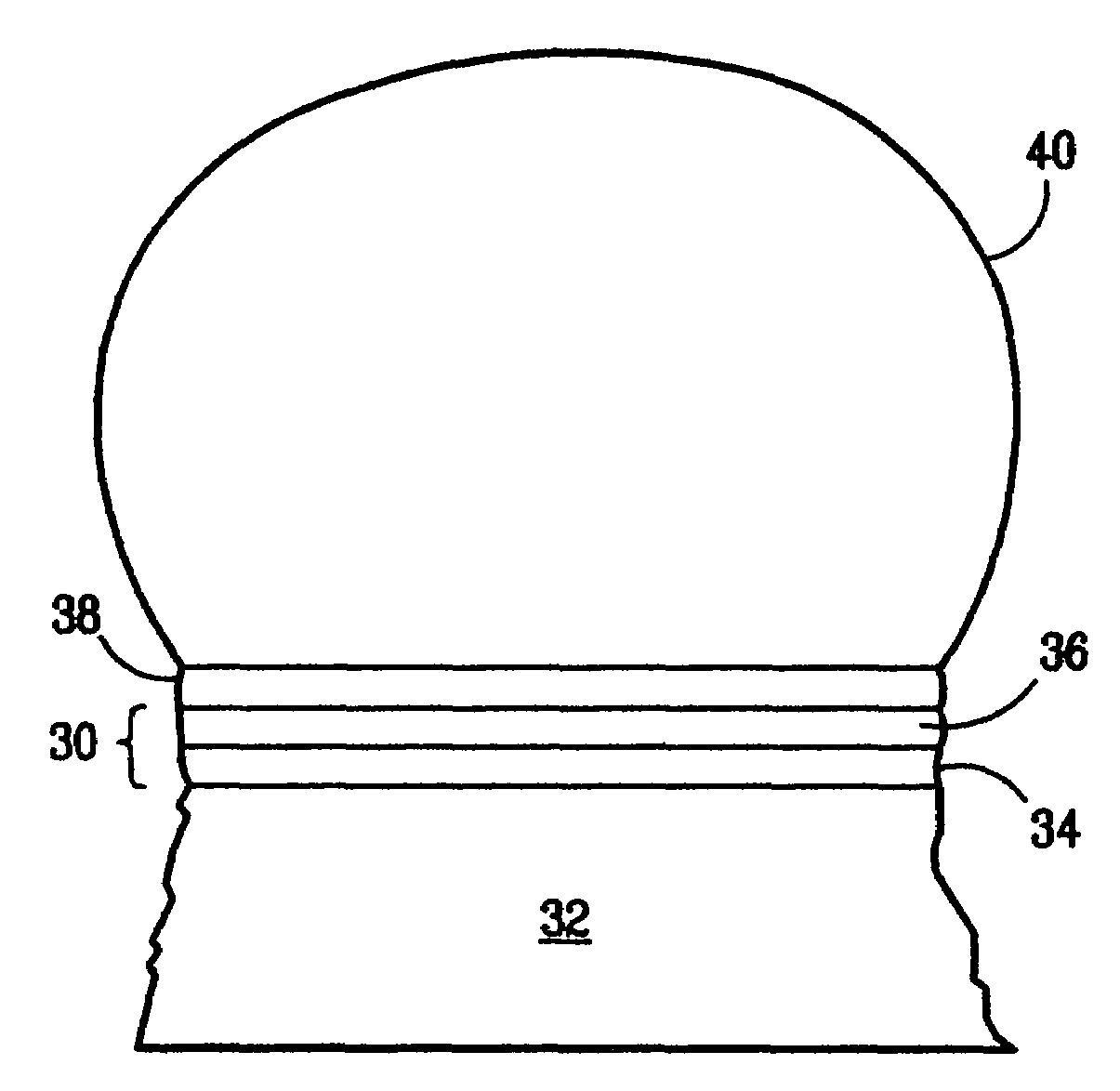
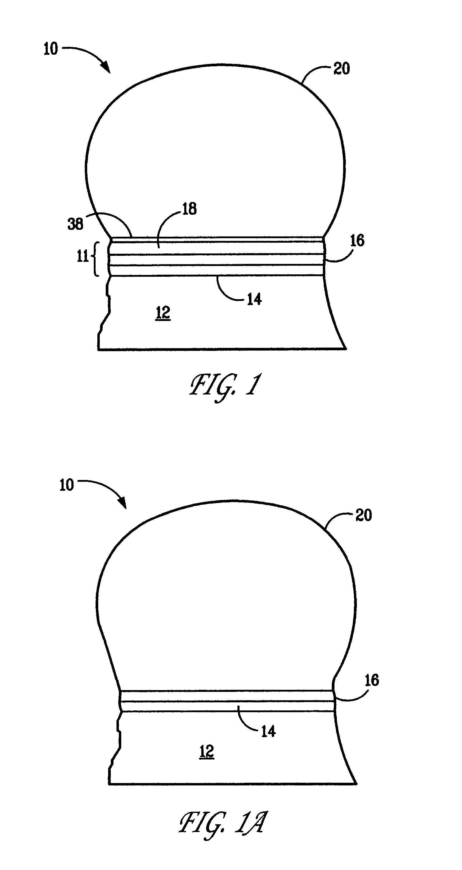
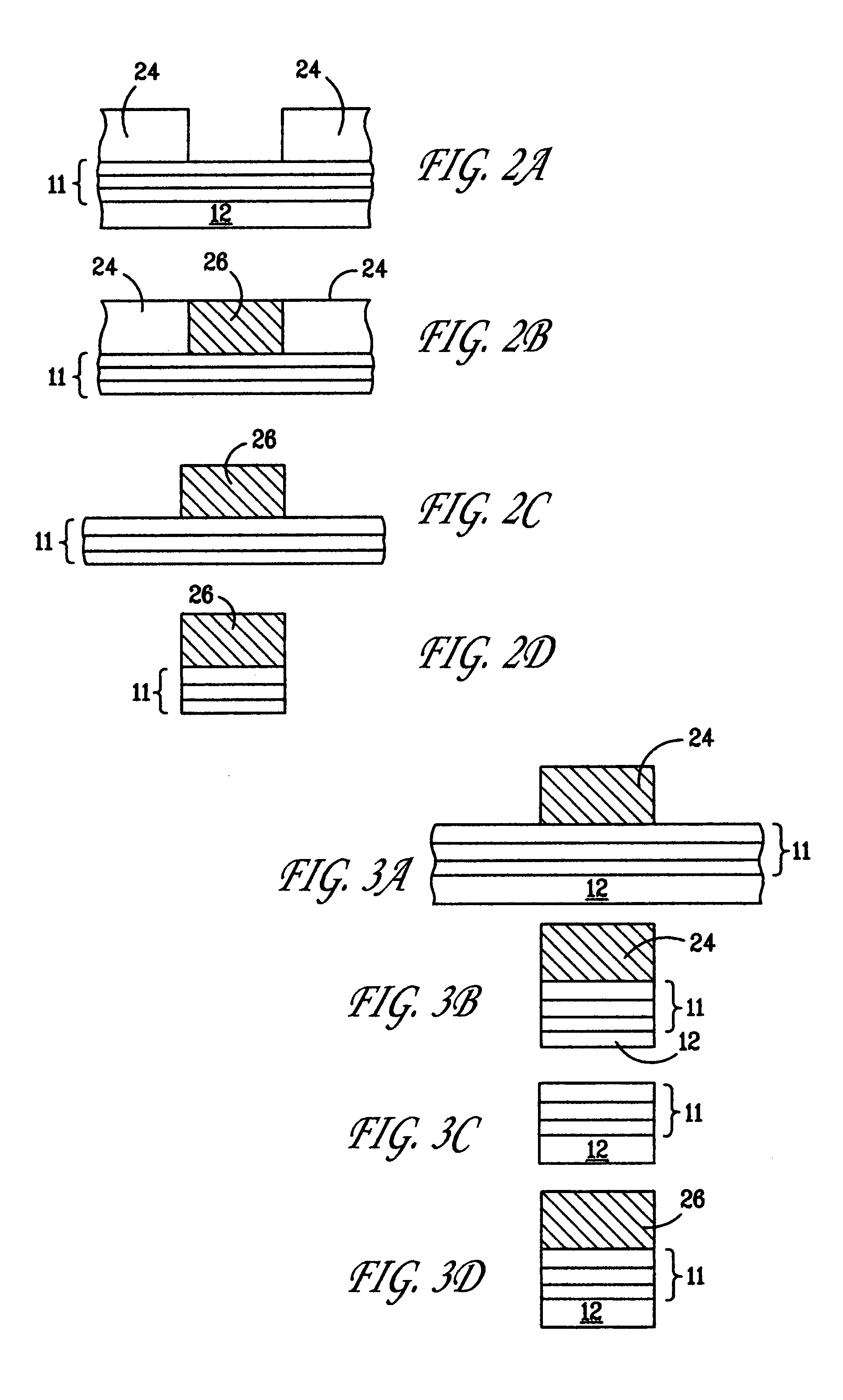
A Three Layer UBM
[0040]In accordance with the present invention, a preferred adhesion layer 14 is Cr, TiW or Ti, which is preferably either sputtered or evaporated, at a preferred thickness of about 100 to 3000 angstroms. The thickness of the adhesion layer 12 can vary widely as long as both good adhesion and good barrier properties are maintained. If blanket TiW is deposited and subsequently etched as the final step in forming the patterned BLM structure 11, the film thickness should be minimized consistent with adequate performance. An alternative adhesion layer is Cr or Ti at a thickness of about 100 to 3000 angstroms.
[0041]The second layer 16 is a solder reaction barrier layer, typically a few thousand angstroms to 2 microns in thickness, deposited by sputtering, evaporation or plating. Since the high tin content Pb-free solders are much more reactive than the Pb-rich PbSn solder alloys, Cu, widely used in the high Pb solder, is shown to form thick tin-copper intermetallics at t...
example 2
A Four Layer UBM
[0047]In this example, the first layer is preferably Cr or TiW. The second layer is preferably Ti, Zr, V, or their alloys (or compounds). The third layer is preferably Cu, CO, Ni, Pd, Pt or their alloys. A fourth layer may be Au or Sn.
example 3
A Simple Two Layer UBM
[0048]In this example, the first layer is preferably Ti which serves both as an adhesion layer and a reaction barrier layer. The second layer is selected from the group consisting of Cu, CO, Ni, Pd, Pt, Sn or their alloys.
[0049]In all three structures Cu is the preferred layer for the reaction, dissolution and incorporation into the solder alloy during reflow joining to form the Sn—Cu or Sn—Ag—Cu solder alloys by simply requiring the plating of the pure Sn or Sn—Ag, respectively, as the bump material.
[0050]The melting properties of the solder alloy that is used over the UBM must be consistent with the requirements of the C4 application. This constraint limits the preferred alloys to those with compositions near the tin-silver eutectic (which contains 2.0-3.8% silver by weight), tin-copper, tin-bismuth, tin-silver-copper ternary eutectic and tin-antimony alloys. The tin-silver eutectic has a melting point of 221 degrees C. and is suitable for this application. H...
PUM
| Property | Measurement | Unit |
|---|---|---|
| thickness | aaaaa | aaaaa |
| thickness | aaaaa | aaaaa |
| thickness | aaaaa | aaaaa |
Abstract
Description
Claims
Application Information