
Low α-dose tin or tin alloy, and method for producing same

a technology low dose, which is applied in the field of tin or tin alloys, can solve the problems of increasing requiring a complex process of removing pb, and the inability to use lower dose, so as to achieve high densification, increase the risk of soft errors, and low operation voltage and cell capacity

Active Publication Date: 2016-07-19
JX NIPPON MINING & METALS CORP
View PDF17 Cites 1 Cited by
  • Summary
  • Abstract
  • Description
  • Claims
  • Application Information

AI Technical Summary

Benefits of technology

The present invention provides a solution to the problem of soft errors in semiconductor devices caused by α rays emitted from materials near the chips. By using tin and tin alloy with low α rays, the occurrence of soft errors can be significantly reduced.

Problems solved by technology

Since recent semiconductor devices are highly densified and of low operation voltage and cell capacity, there is an increasing risk of soft errors caused by the influence of α rays emitted from materials in the vicinity of semiconductor chips.
However, this method requires a complex process of removing Pb after being added to tin.
Furthermore, the refined tin showed a significantly lower α dose in three years after refining; however, it can also be interpreted that the tin with a lower α dose cannot be used until three years later.
Accordingly, this method is not considered to be industrially efficient.
However, even with the addition of such materials, the radiation α particle count could be reduced only to a level of 0.015 cph / cm2, which does not reach the level expected for current semiconductor device materials.
Another problem is that alkali metal elements, transition metal elements, heavy metal elements, and other elements that are undesirably mixed in semiconductors are used as the materials to be added.
However, this level of count of radiation α particles does not reach the level expected for current semiconductor device materials.
Nevertheless, the lowest α-ray count of the deposited tin shown in an Example of Document 4 is 0.002 cph / cm2, which does not reach the expected level, despite the high cost.
Thus, Document 5 lacks interest in these limitations.
In this case, however, even though the amount of Pb is reduced as much as possible, no means are provided to fundamentally solve the problem of the radiation α particle count caused by the Pb being inevitably incorporated.
Nevertheless, the lowest α-ray count of the deposited tin shown in an Example of Document 7 is 0.003 cph / cm2, which does not reach the expected level, despite the high cost.
In Document 8 and Document 9, allowable values concerning the radiation α particle count are respectively lenient, and there is a problem in that the techniques of these documents do not reach the level expected for current semiconductor device materials.

Method used

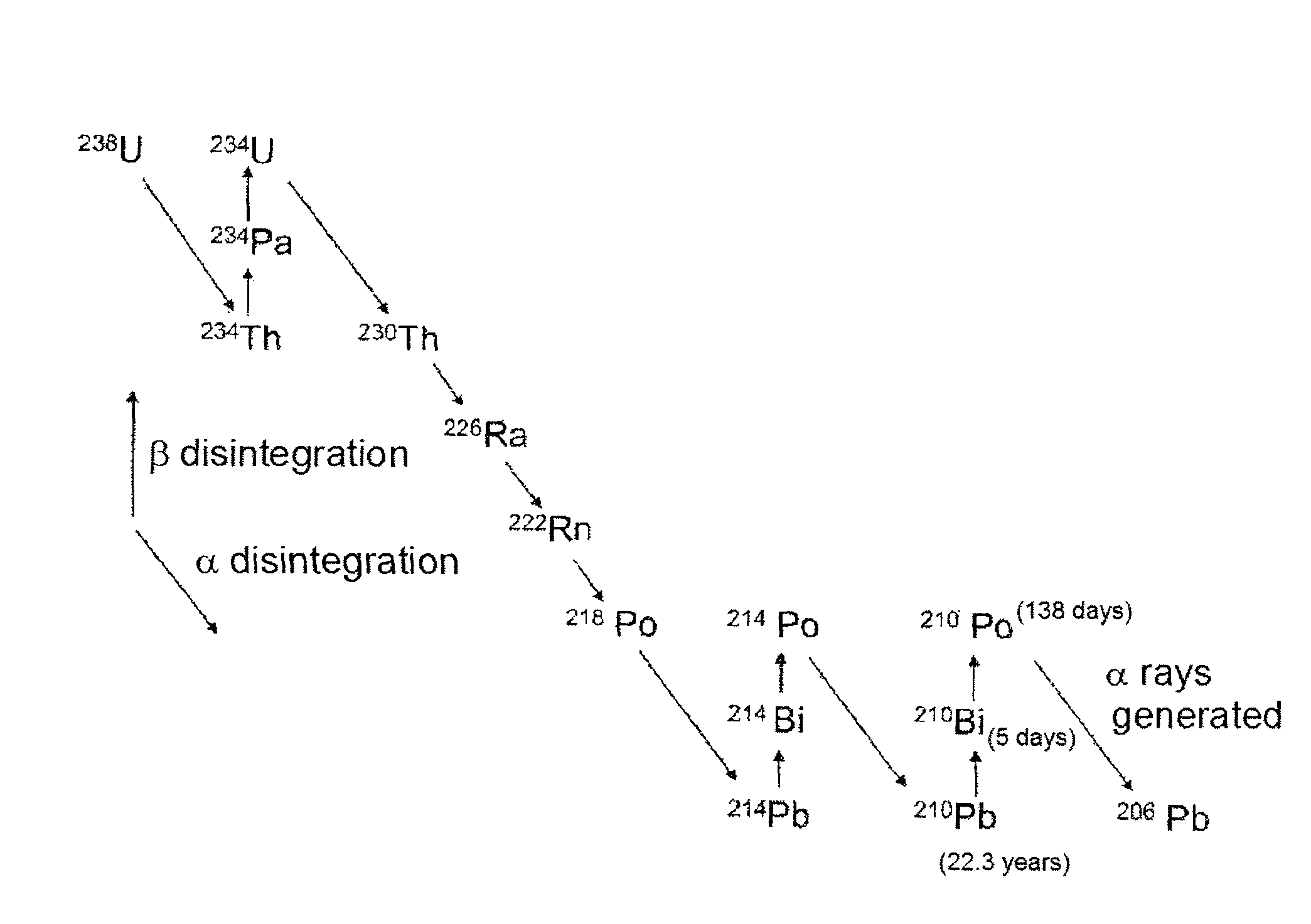

Image

  • Low α-dose tin or tin alloy, and method for producing same
  • Low α-dose tin or tin alloy, and method for producing same
  • Low α-dose tin or tin alloy, and method for producing same

Examples


example 1

[0060]Raw material tin with a purity level of 3N was leached in hydrochloric acid (or sulfuric acid), and the resulting leachate having a pH of 1.0 and an Sn concentration of 80 g / L was used as an electrolyte. Using a tin plate obtained by casting raw material tin as the anode, and a titanium plate as the cathode, electrolysis was carried out under conditions where the electrolysis temperature was 30° C., and the current density was 7 A / dm2.

[0061]When the thickness of the tin electrodeposited on the cathode reached about 2 mm, the electrolysis was halted, and the cathode was taken out from the electrolytic cell. The electrodeposited tin was collected by being removed from the cathode. After the collection, the cathode was returned to the electrolytic cell, and the electrolysis was started again. This operation was repeated. The collected electrodeposited tin was washed and dried, and melted and cast at a temperature of 260° C. to obtain a tin ingot.

[0062]The tin ingot was subject to...

example 2

[0069]Raw material tin with a purity level of 3N was leached in hydrochloric acid (or sulfuric acid), and the resulting leachate having a pH of 1.0 and an Sn concentration of 80 g / L was used as an electrolyte. Using a tin plate obtained by casting raw material tin as the anode, and a titanium plate as the cathode, electrolysis was carried out under conditions where the electrolysis temperature was 30° C., and the current density was 1 A / dm2.

[0070]When the thickness of the tin electrodeposited on the cathode reached about 2 mm, the electrolysis was halted, and the cathode was taken out from the electrolytic cell. The electrodeposited tin was collected by being removed from the cathode. After the collection, the cathode was returned to the electrolytic cell, and the electrolysis was started again. This operation was repeated. The collected electrodeposited tin was washed and dried, and melted and cast at a temperature of 260° C. to obtain a tin ingot.

[0071]The tin ingot was subject to...

example 3

[0077]Raw material tin with a purity level of 3N was leached in hydrochloric acid (or sulfuric acid), and the resulting leachate having a pH of 1.0 and an Sn concentration of 80 g / L was used as an electrolyte.

[0078]Using a tin plate obtained by casting raw material tin as the anode, and a titanium plate as the cathode, electrolysis was carried out under conditions where the electrolysis temperature was 30° C., and the current density was 1 A / dm2.

[0079]When the thickness of the tin electrodeposited on the cathode reached about 2 mm, the electrolysis was halted, and the cathode was taken out from the electrolytic cell. The electrodeposited tin was collected by being removed from the cathode. After the collection, the cathode was returned to the electrolytic cell, and the electrolysis was started again. This operation was repeated. The collected electrodeposited tin was washed and dried, and melted and cast at a temperature of 260° C. to obtain a tin ingot.

[0080]The tin ingot was subje...


PUM

PropertyMeasurementUnit
pHaaaaaaaaaa
concentrationaaaaaaaaaa

Abstract

Disclosed is tin characterized in that a sample of the tin after melting and casting has an α dose of less than 0.0005 cph / cm2. Since recent semiconductor devices are highly densified and of high capacity, there is an increasing risk of soft errors caused by the influence of α rays emitted from materials in the vicinity of semiconductor chips. In particular, there are strong demands for high purification of solder materials and tin for use in the vicinity of semiconductor devices, and demands for materials with lower α rays. Accordingly, an object of the present invention is to clarify the phenomenon of the generation of α rays in tin and tin alloys, and to obtain high-purity tin, in which the α dose has been reduced, suitable for the required materials, as well as a method for producing the same.

Description

BACKGROUND[0001]The present invention relates to tin or tin alloys, in which the α (alpha) dose has been reduced, for use in the production of semiconductors, etc., and a method for producing the same.[0002]Generally, tin is a material used in the production of semiconductors, and is particularly a main raw material for solder materials. In the production of semiconductors, when a semiconductor chip and a substrate are bonded, and an Si chip, such as IC or LSI, is bonded to or sealed in a lead frame or a ceramics package, solder is used to form bumps during TAB (tape automated bonding) or during the manufacture of flip chips, and is used as a semiconductor wiring material.[0003]Since recent semiconductor devices are highly densified and of low operation voltage and cell capacity, there is an increasing risk of soft errors caused by the influence of α rays emitted from materials in the vicinity of semiconductor chips. For this reason, there are demands for high purification of the af...

Claims


Application Information

Patent Timeline
Patent Type & Authority Patents(United States)
IPC IPC(8): C25C1/14B23K35/36B23K35/26B23K35/40C22C13/00
CPCC22C13/00B23K35/262B23K35/36B23K35/40B23K2201/40B23K2101/40C22B25/08B23K35/26C22B3/04
Inventor KANOU, GAKU
Owner JX NIPPON MINING & METALS CORP
Learn More