Image sensor assembly and method for fabricating the same

a technology of image sensor and assembly method, which is applied in the direction of radiation control devices, semiconductor devices, semiconductor/solid-state device details, etc., can solve the problems of difficult to fabricate traces on the double layer and side of glass substrate, image sensor chip lack of protection, and high fabrication cost of glass substrate. achieve the effect of reducing the overall package thickness

Inactive Publication Date: 2008-09-02
CHIPMOS TECH INC
View PDF5 Cites 9 Cited by
  • Summary
  • Abstract
  • Description
  • Claims
  • Application Information

AI Technical Summary

Benefits of technology

[0004]The main purpose of the present invention is to provide an assembly device and an assembling method for an image sensor chip using a bent flexible circuit to protect the sides of the image sensor chip. The flexible circuit has a plurality of bendable portions extending from a die-attached portion and connecting to a plurality of bonding portions. The bendable portions are bent to locate around the sides of the image sensor chip, the bonding portions are located above the image sensor chip. A plurality of inner leads formed on the bonding portions are bonded to the bumps on the image sensor chip. The bent bendable portions can protect the image sensor chip to replace the conventional encapsulant and reduce the overall package thickness.
[0005]According to the present invention, an image sensor assembly mainly comprises a flexible circuit and an image sensor chip having bumps. The flexible circuit has a die-attached portion, a plurality of bendable portions, and a plurality of bonding portions where the bendable portions are extended from the die-attached portion and are connected to the bonding portions respectively. A plurality of inner leads are formed on the bonding portions. An image sensor chip is attached to the die-attached portion of the flexible circuit where the image sensor chip has a sensing area where the bumps are formed around the sensing area on the image sensor chip. The bendable portions are so bent that the bonding portions are located above the image sensor chip and the bendable portions are located around sides of the image sensor chip. Thereby, the inner leads of the bonding portions can be bonded to the bumps on the image sensor chip. Preferably, a transparent cover is adhered to the bonding portions corresponding to the sensing area of the image sensor chip to prevent moisture or dusts contaminating the sensing area. A plurality of solder balls may be placed on the flexible circuit.

Problems solved by technology

However, it is very difficult to fabricate traces on double layers and sides of the glass substrate.
Accordingly, the fabrication cost of the glass substrate is very high.
Moreover, the image sensor chip is lack of protection.
The sensing area of the image sensor chip is easily contaminated during molding the encapsulant and the total thickness of the image sensor package cannot be reduced.

Method used


Image

  • Image sensor assembly and method for fabricating the same
  • Image sensor assembly and method for fabricating the same
  • Image sensor assembly and method for fabricating the same

Examples


first embodiment

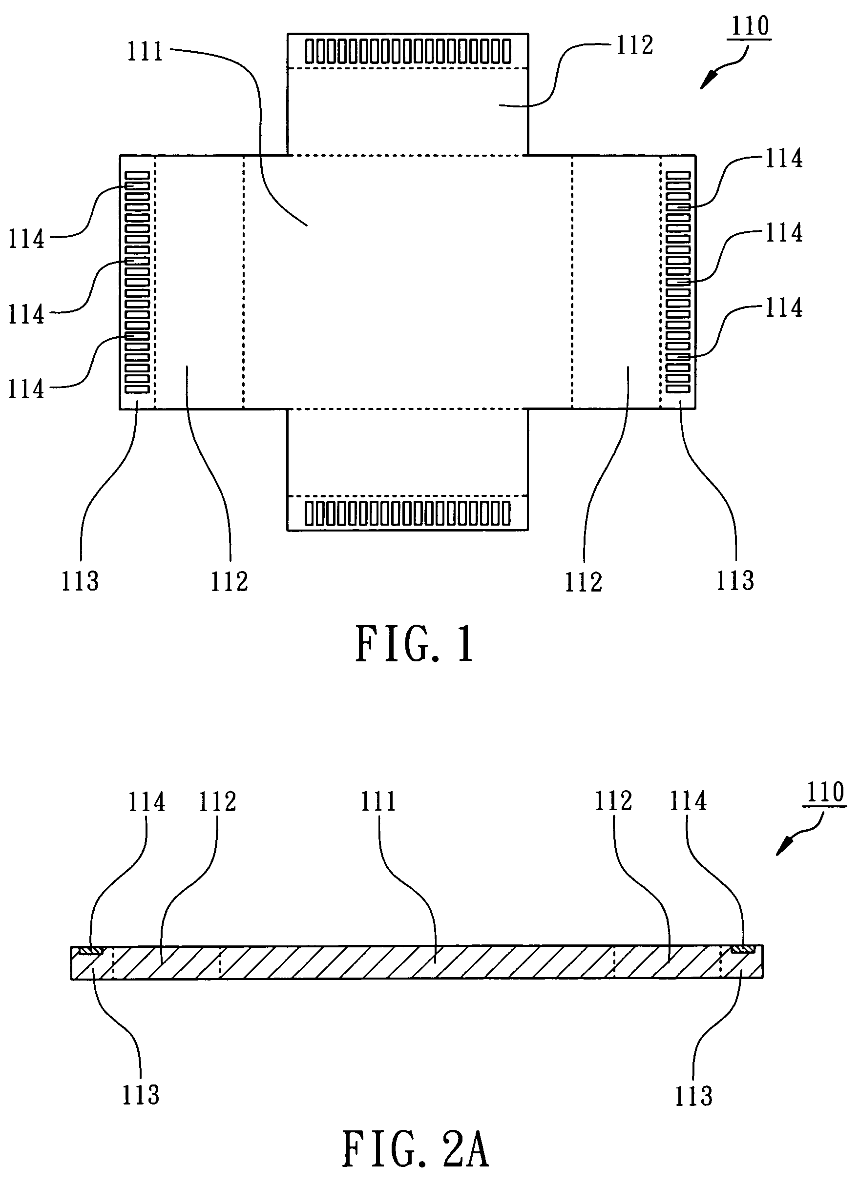
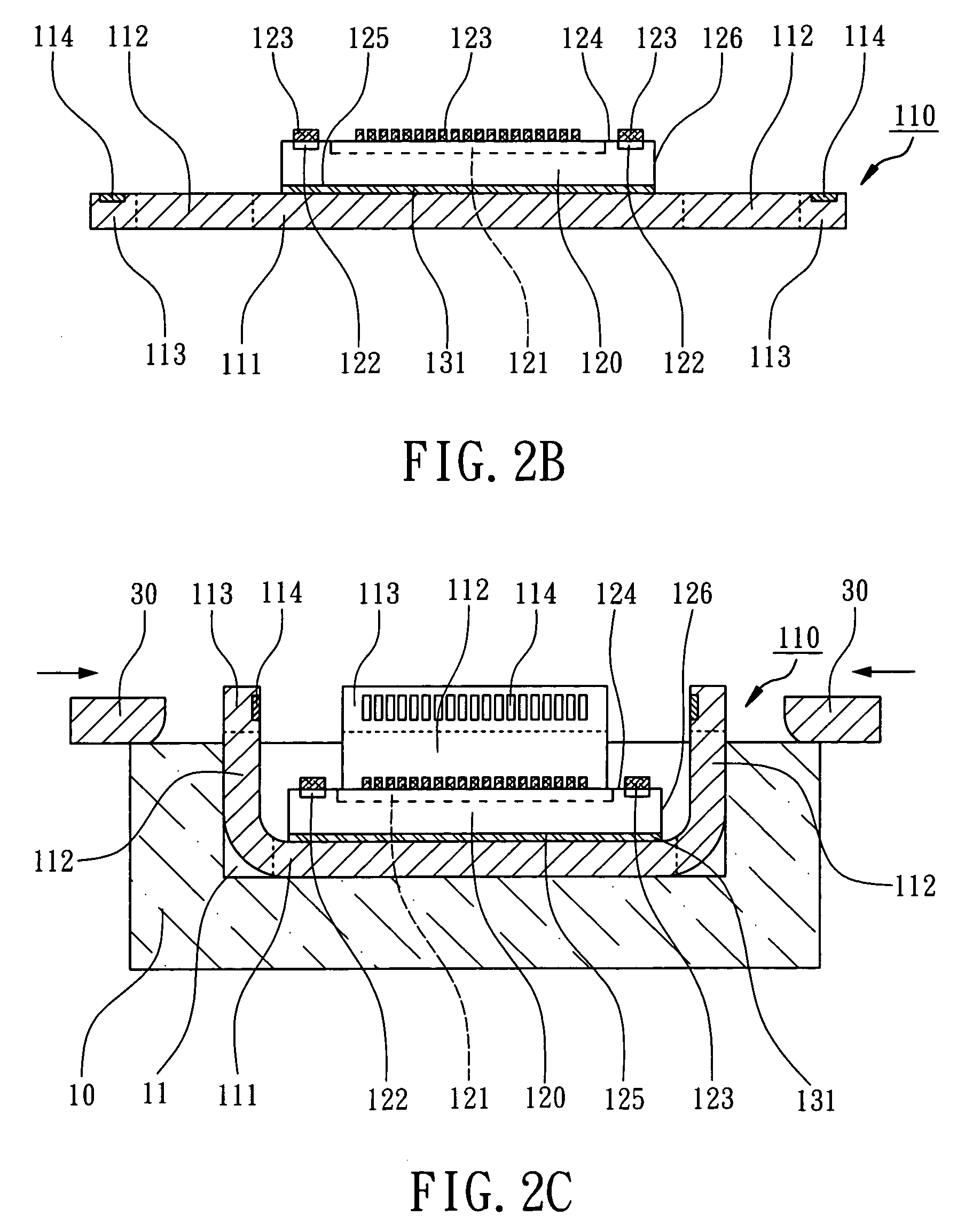
[0011]According to the present invention, FIG. 1 shows a flexible circuit for an image sensor assembly, FIG. 2A to 2F show the flexible circuit during assembling processes, especially FIG. 2F shows the cross-sectional view of the image sensor assembly. The image sensor assembly mainly comprises a flexible circuit 110 and an image sensor chip 120. As shown in FIGS. 1 and 2A, the flexible circuit 110 has a die-attached portion 111, a plurality of bendable portions 112 and a plurality of bonding portions 113 where the bendable portions 112 are extended from the die-attached portion 111 and are connected to the bonding portions 113 respectively. The flexible circuit 110 which is made of a polyimide (PI) film with a thickness not greater than 0.2 mm and has at least a wiring layer. A plurality of inner leads 114 are formed on the bonding portions 113 where the inner leads 114 are made of copper metal foil, preferably, a nickel / gold layer is disposed on the inner leads 114 (not shown in t...

second embodiment

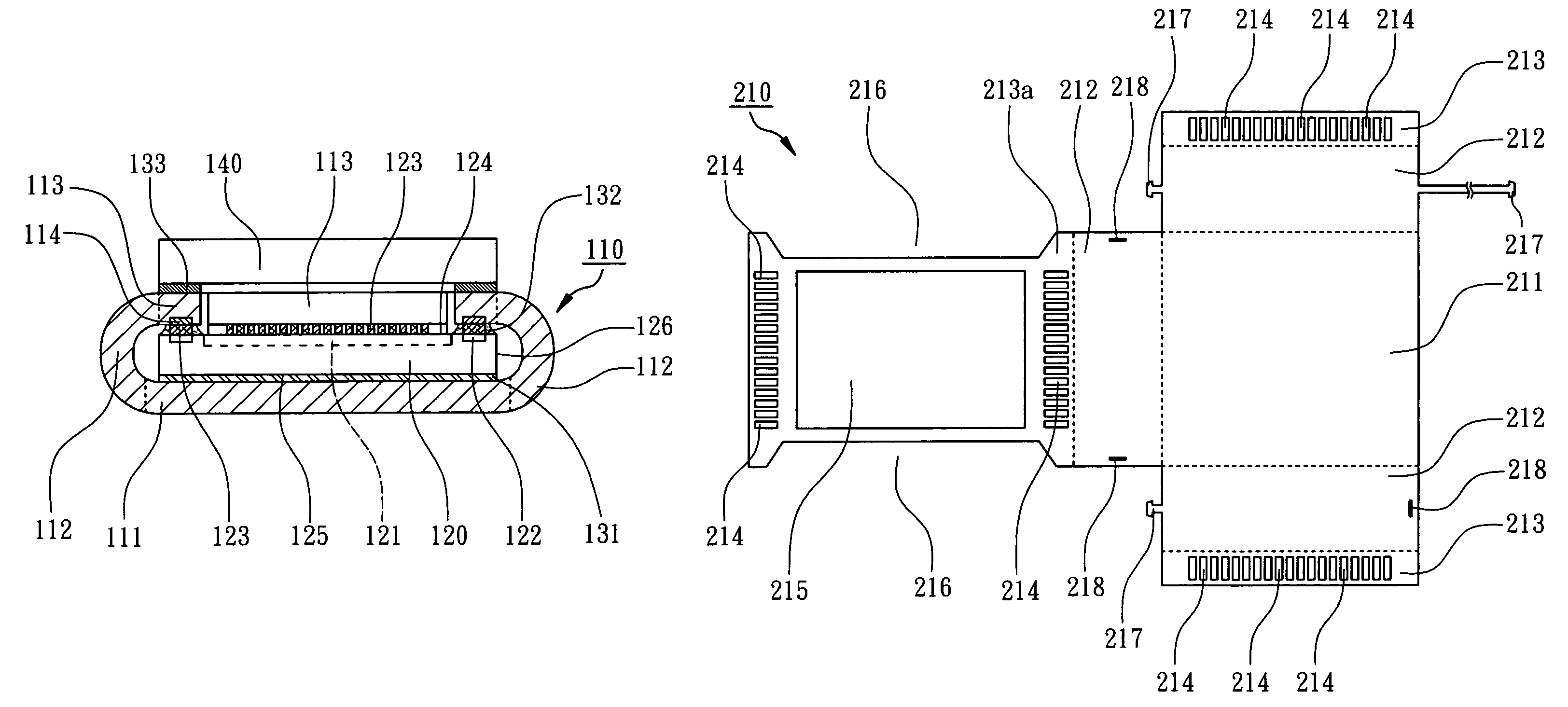
[0018]According to the present invention, FIG. 3 shows another flexible circuit for an image sensor assembly, FIG. 4A to 4E show the flexible circuit during assembling processes, especially FIG. 4E shows the cross-sectional view of the image sensor assembly. The image sensor assembly mainly comprises a flexible circuit 210 and an image sensor chip 220. As shown in FIGS. 3 and 4A, the flexible circuit 210 has a die-attached portion 211, a plurality of bendable portions 212, and a plurality of bonding portions 213 where the bendable portions 212 are extended from the die-attached portion 211 and are connected to the bonding portions 213. A plurality of inner leads 214 are formed on the bonding portions 213. One bonding portion 213a of the bonding portions 213 has an opening 215. The opening 215 is aligned with a sensing area 221 of the image sensor chip 220 after thermocompression bonding the bonding portions 213 to the image sensor chip 220 (as shown in FIG. 4E). In this embodiment, ...


PUM


Abstract

An assembly device of an image sensor chip is disclosed. A flexible circuit has a die-attached portion, a plurality of bendable portions, and a plurality of bonding portions where the bendable portions extend from the die-attached portion and are connected to the corresponding bonding portions. A plurality of inner leads are formed on the bonding portions. An image sensor chip with bumps is attached to the die-attached portion. The bendable portions are so bent that the bonding portions are located above the image sensor chip. By thermocompression bonding, the inner leads of the flexible circuit are bonded to the bumps on the image sensor chip. In one embodiment, a transparent cover is adhered to the bonding portions and located above a sensing area of the image sensor chip.

Description

FIELD OF THE INVENTION[0001]The present invention relates to an assembly device of an image sensor chip and its fabricating method, and more particularly, to an assembly device of an image sensor chip using flexible circuit to replace the conventional rigid substrate and the encapsulant.BACKGROUND OF THE INVENTION[0002]Image sensor chips have been widely implemented in everyday lives such as cellular phones, personal digital assistants (PDA), digital still cameras (DSC), digital video cameras (DV), video phones, video conferences, and so on. It is necessary to packaging image sensor chips prior to surface-mounting. A disclosed image sensor package and its packaging method are revealed in R.O.C. Taiwan patent publication No. 459,355. An image sensor chip is flip-chip bonded to a glass substrate. A plurality of signal input terminals and a plurality of signal output terminals, which are formed on the different surfaces of the glass substrate, are electrically connected to each other b...

Claims


Application Information

Patent Timeline
Patent Type & Authority Patents(United States)
IPC IPC(8): H01L23/02H01L23/28H01L27/146
CPCH01L27/14618H01L27/14685H01L27/14636H01L2924/0002H01L2924/00
Inventor CHAO, YEONG-CHINGLIU, AN-HONGLEE, YAO-JUNG
Owner CHIPMOS TECH INC
Why Eureka
Try Eureka