Light-receiving amplifier and optical pickup device

a pickup device and amplifier circuit technology, applied in the direction of gain control, record information storage, instruments, etc., can solve the problems of small output voltage range (dynamic range) extreme poor s/n ratio of output signals of the light-receiving amplifier circuit, etc., to avoid narrowing down of the output voltage range, reduce heat noise, and prevent deterioration of the s/n ratio

Inactive Publication Date: 2008-09-23
SHARP KK
View PDF9 Cites 6 Cited by
  • Summary
  • Abstract
  • Description
  • Claims
  • Application Information

AI Technical Summary

Benefits of technology

[0024]The present invention is made in view of the foregoing problem, and it is an object of the present invention to provide a light-receiving amplifier circuit and an optical pickup device each capable of reducing heat noise and preventing deterioration in the S / N ratio, while avoiding narrowing down of the output voltage range (dynamic range).
[0026]In the configuration, the first preamplifier is provided with the output voltage expanding circuit for supplying the output voltage range from the amplifier to the differential amplifier circuit. This output voltage expanding circuit is connected to (i) the other end of at least one of plural feedback resistors in the first preamplifier and (ii) the output terminal of the amplifier. This configuration allows expansion of output voltage range to be supplied from the amplifier of the first preamplifier to the differential amplifier circuit. Accordingly, setting of the amplification factor of the differential amplifier circuit at less than 1, for the purpose of reducing heat noise in the light-receiving amplifier circuit, does not cause narrowing down of the output voltage range of the differential amplifier circuit. Thus, it is possible to reduce the heat noise to prevent deterioration of the S / N ratio, while avoiding narrowing down of the output voltage range of the light-receiving amplifier.
[0028]The above configuration is provided with the output voltage expanding circuit for expanding the output voltage range from the differential amplifier and for supplying the expanded output voltage range to the differential amplifier circuit. This output voltage expanding circuit is connected to the other end of at least one of the plural feedback resistors and the output terminal of the differential amplifier. This configuration allows expansion of output voltage range to be supplied from the differential amplifier of the pre-differential amplifier to the differential amplifier circuit. Accordingly, setting of the amplification factor of the differential amplifier circuit at less than 1, for the purpose of reducing heat noise in the light-receiving amplifier circuit, does not cause narrowing down of the output voltage range of the differential amplifier circuit. Thus, it is possible to reduce the heat noise to prevent deterioration of the S / N ratio, while avoiding narrowing down of the output voltage range of the light-receiving amplifier.
[0030]In the above configuration, the light-receiving amplifier circuit is provided with the output voltage expanding circuit for expanding the output voltage range from the differential amplifier and for supplying the expanded output voltage range to the differential amplifier circuit. This output voltage expanding circuit is connected to the other end of at least one of the plural feedback resistors and the output terminal of the differential amplifier. This configuration allows expansion of output voltage range to be supplied from the differential amplifier of the pre-differential amplifier to the differential amplifier circuit. Accordingly, setting of the amplification factor of the differential amplifier circuit at less than 1, for the purpose of reducing heat noise in the light-receiving amplifier circuit, does not cause narrowing down of the output voltage range of the differential amplifier circuit. Thus, it is possible to reduce the heat noise to prevent deterioration of the S / N ratio, while avoiding narrowing down of the output voltage range of the light-receiving amplifier.

Problems solved by technology

This causes an extremely poor S / N ratio of output signals Vo of the light-receiving amplifier circuit 91.
In such a conventional circuit, however, the reduction of the gain (Rf94 / Rs92) of the differential amplifier circuit 98 to less than 1 causes a problem of smaller output voltage range (dynamic range) of the light-receiving amplifier circuit, than a case where the gain is 1 or more.

Method used


Image

  • Light-receiving amplifier and optical pickup device
  • Light-receiving amplifier and optical pickup device
  • Light-receiving amplifier and optical pickup device

Examples


embodiment 1

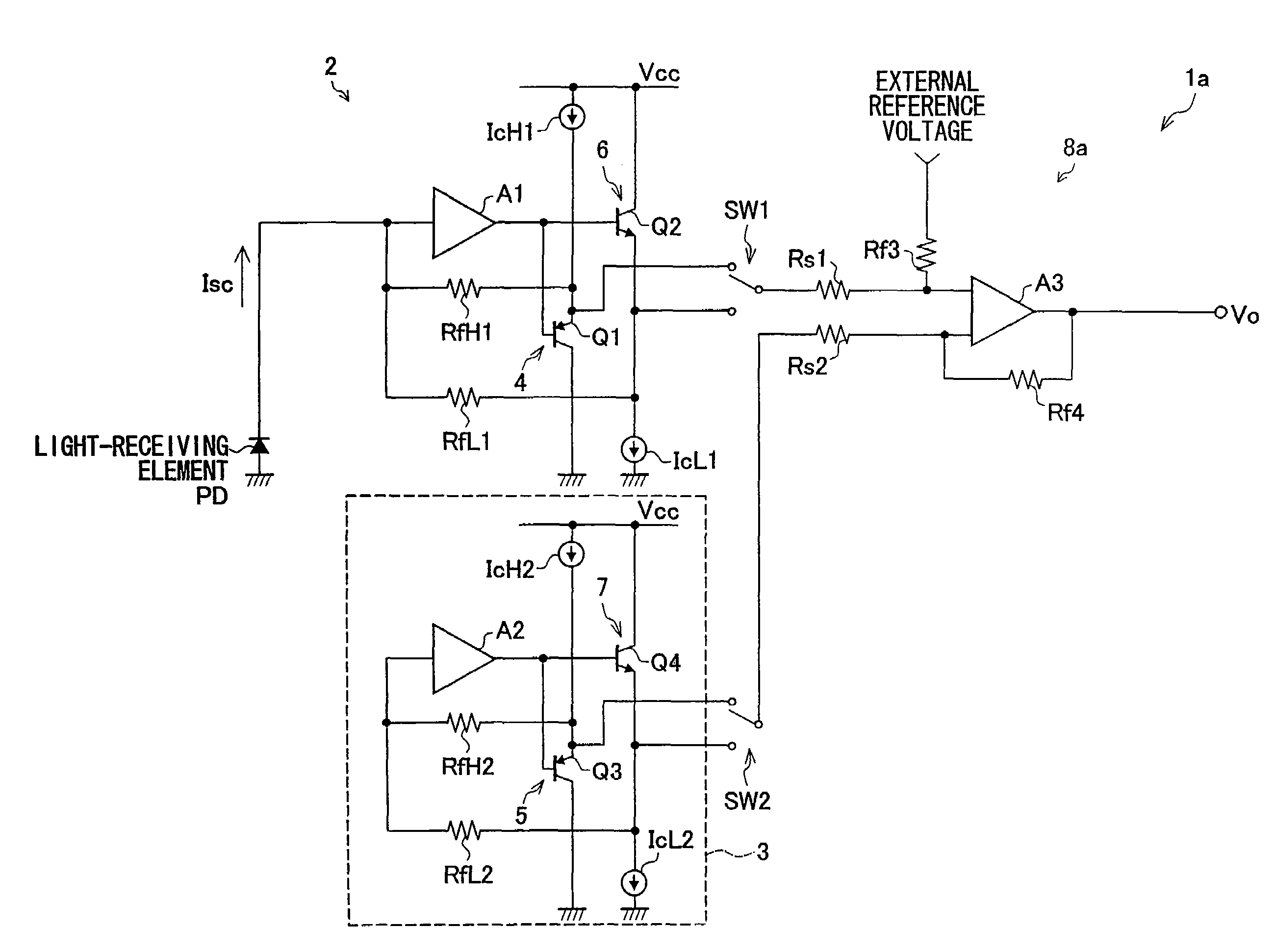
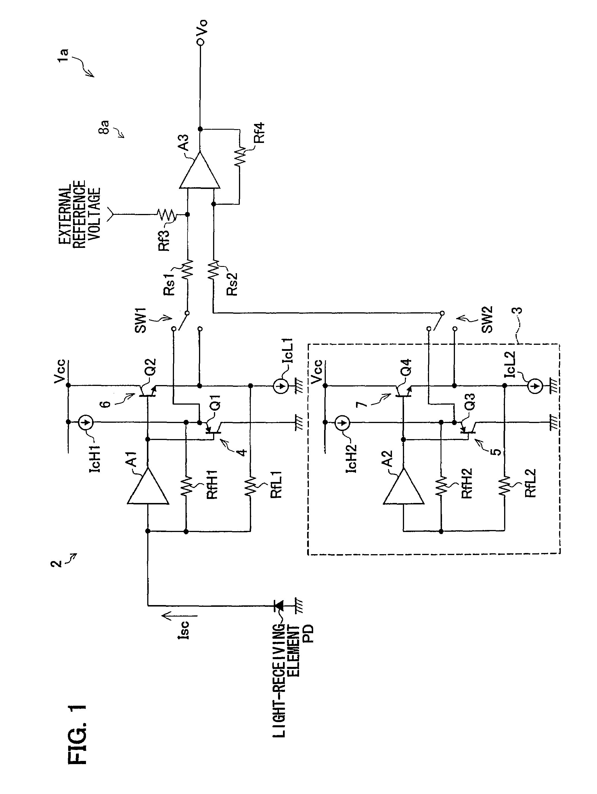
[0042]FIG. 1 is a circuit diagram illustrating a configuration of a light-receiving amplifier circuit 1a of Embodiment 1. The light-receiving amplifier circuit 1a is provided with a preamplifier circuit 2 including an amplifier A1. To an input terminal of this amplifier A1 connected is one end of a light-receiving element PD whose another end is grounded. The amplifier A1 includes feedback resistors RfH1 and RfL1 for use in current-voltage conversion, each of which resistors provided so that feedback resistors RfH91 and RfL91 and the amplifier A91 are connected in parallel to one another. One end of each of the feedback resistors RfH1 and RfL1 is commonly connected to the input terminal of the amplifier A1.

[0043]The preamplifier circuit 2 is further provided with an emitter follower circuit (output voltage expanding circuit) 4 which includes a PNP transistor Q1 and a constant current source IcH1. The gate of the PNP transistor Q1 is connected to an output terminal of the amplifier A...

embodiment 2

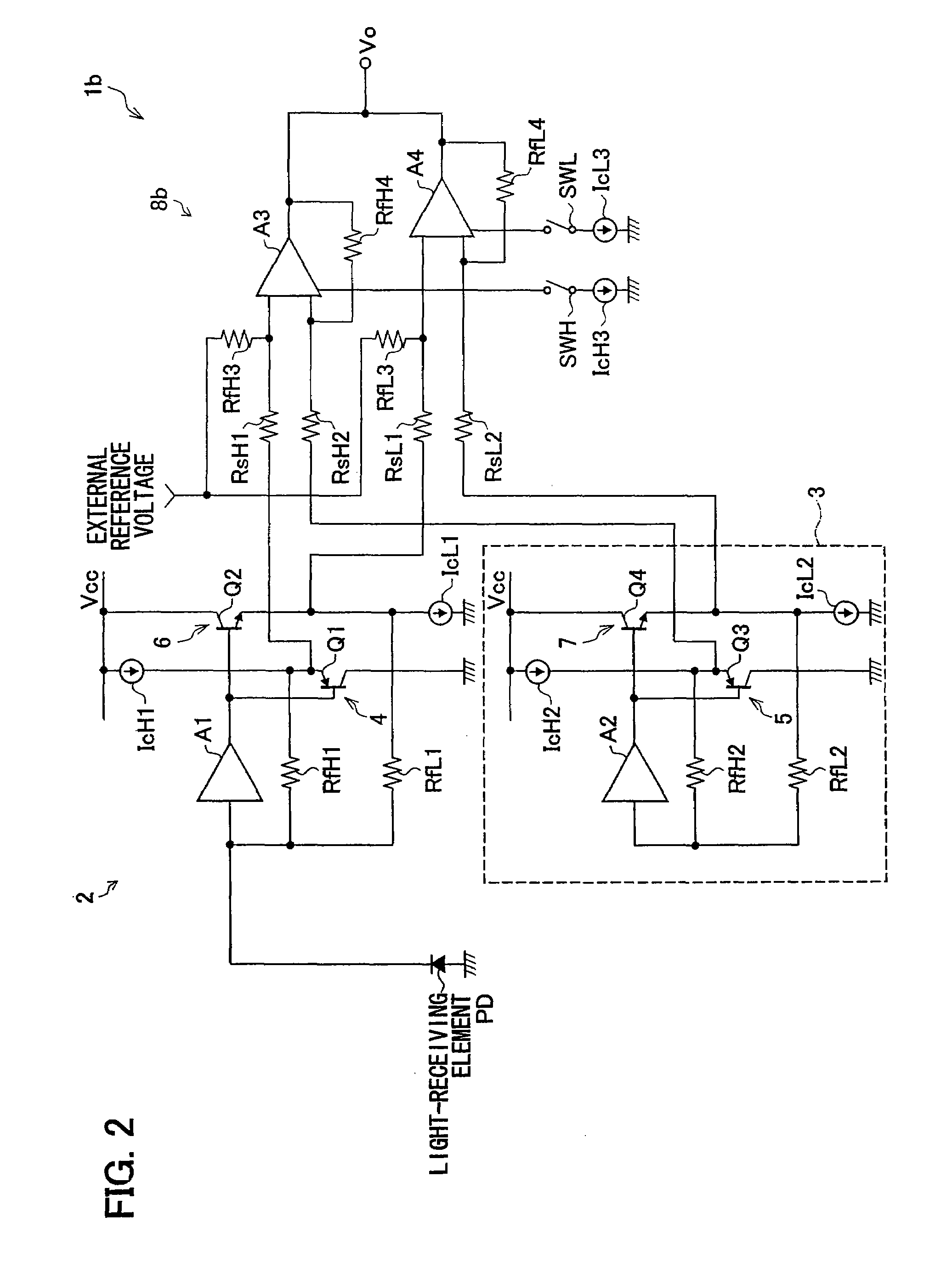
[0064]FIG. 2 is a circuit diagram illustrating a configuration of a light-receiving amplifier circuit 1b of Embodiment 2. The same symbols are given to members which are identical to those of the foregoing configuration, and detailed explanation for these members are omitted. The same goes for the rest of the embodiments.

[0065]The light-receiving amplifier circuit 1b is provided with a differential amplifier circuit 8b which includes two differential amplifiers (first and second differential amplifiers) A3 and A4 connected in parallel to each other. One of the input terminals (first input terminal) of the differential amplifier A3 is connected, via a resistor RsH1, to a connection point between a PNP transistor Q1 and a constant current source IcH1 of a preamplifier circuit 2. Another one of the input terminals (second input terminal) of the differential amplifier A3 is connected, via a resistor RsH2, to a connection point between a PNP transistor Q3 and a constant current source Ic...

embodiment 3

[0069]FIG. 3 is a circuit diagram illustrating a configuration of a light-receiving amplifier circuit 1c of Embodiment 3. The light-receiving amplifier circuit 1c is an example where a grounded amplifier is used as an amplifier of a preamplifier circuit.

[0070]The light-receiving amplifier circuit 1c is provided with a preamplifier circuit 2c. The preamplifier circuit 2c has an NPN transistor Q5. The base of the NPN transistor Q5 is connected to: (i) a light-receiving element PD; (ii) one end of a feedback resistor RfH1; and (iii) one end of a feedback resistor RfL1. The collector of the NPN transistor Q5 is connected to: (i) the bases of a PNP transistor Q1 and an NPN transistor Q2; and (ii) one end of a constant current source Ic1 whose another end is connected to a line through which a power source voltage Vcc is supplied. The emitter of the NPN transistor Q5 is grounded.

[0071]The light-receiving amplifier circuit 1c further includes a preamplifier circuit 3c which includes an NPN...


PUM

PropertyMeasurementUnit
output voltageaaaaaaaaaa
voltageaaaaaaaaaa
resistanceaaaaaaaaaa

Abstract

A light-receiving amplifier circuit of the present invention includes: a first preamplifier circuit to which a light-receiving element is connected; a second preamplifier circuit which is the same type as the first preamplifier circuit and which is apart from the light-receiving element; and a differential amplifier circuit for amplifying output voltage differential between the preamplifier circuits, wherein each of the first preamplifier circuit includes an amplifier and first and second plural feedback resistors, each of which resistors has an end commonly connected to an input terminal of the amplifier; an amplification factor of the differential amplifier circuit is less than one; and the first preamplifier circuit includes an output voltage expanding circuit which is connected to (i) another end of the first feedback resistors in the first preamplifier circuit and (ii) an output terminal of the amplifier, and which circuit is for expanding an output voltage range from the amplifier and supplying the expanded output voltage range to the differential amplifier circuit. This configuration provides a light-receiving circuit which is capable of reducing heat noise to prevent deterioration of the S / N ratio, while avoiding narrowing down of an output voltage range.

Description

[0001]This Nonprovisional application claims priority under 35 U.S.C. § 119(a) on Patent Application No. 317553 / 2005 filed in Japan on Oct. 31, 2005, the entire contents of which are hereby incorporated by reference.FIELD OF THE INVENTION[0002]The present invention relates to a light-receiving amplifier circuit and an optical pickup device, each for use in a device capable of reading and / or writing into information to / from an optical disc.BACKGROUND OF THE INVENTION[0003]Optical discs are widely used as a medium for storing therein pieces of data of music, video, documents, or the like, and various devices for reading or writing information from / to an optical disc are developed. Such devices, in many cases, adopts an optical pickup device (See for example Japanese Unexamined Patent Publication No. 2003-187484 (Tokukai 2003-187484; Published on Jul. 4, 2003)) which device is a main element for inputting / outputting signals, by using its edge portion, to / from an optical disc.[0004]FIG....

Claims


Application Information

Patent Timeline
Patent Type & Authority Patents(United States)
IPC IPC(8): H03F3/08G11B7/00
CPCH03F3/08
Inventor SUGIMOTO, KOHICHIROH
Owner SHARP KK
Why Eureka
Try Eureka