Semiconductor device and manufacturing method thereof

a semiconductor and manufacturing method technology, applied in the direction of semiconductor devices, electrical appliances, transistors, etc., can solve the problems of reducing contact resistance, increasing parasitic resistance, inversely increasing parasitic resistance, etc., and achieve the effect of increasing parasitic resistan

Inactive Publication Date: 2008-10-07
FUJITSU SEMICON LTD
View PDF19 Cites 16 Cited by
  • Summary
  • Abstract
  • Description
  • Claims
  • Application Information

AI Technical Summary

Benefits of technology

[0008]Therefore, the present invention is made in view of the aforementioned problem, and it is an object of the invention to provide a semiconductor device and a method of manufacturing thereof capable of making it possible to obtain a sharp impurity profile through the use of the laser annealing method without presenting a disadvantage such as an increase in parasitic resistance or the like, so as to make it possible to meet sufficiently the requirements for making a semiconductor element finer and more highly integrated.

Problems solved by technology

However, the sharp impurity extension obtained by the laser annealing has a disadvantage in that the impurity extension region in the vicinity of a gate electrode which is a mask during ion implantation is strictly defined because the impurity profile is too sharp, which inversely increases its parasitic resistance.
As described above, the use of the laser annealing method provides this sharp impurity profile due to the activating process in a very short period of time which greatly contributes to a reduction in the contact resistance and so on, but conversely presents a serious problem in the increase in parasitic resistance.

Method used


Image

  • Semiconductor device and manufacturing method thereof
  • Semiconductor device and manufacturing method thereof
  • Semiconductor device and manufacturing method thereof

Examples


first embodiment

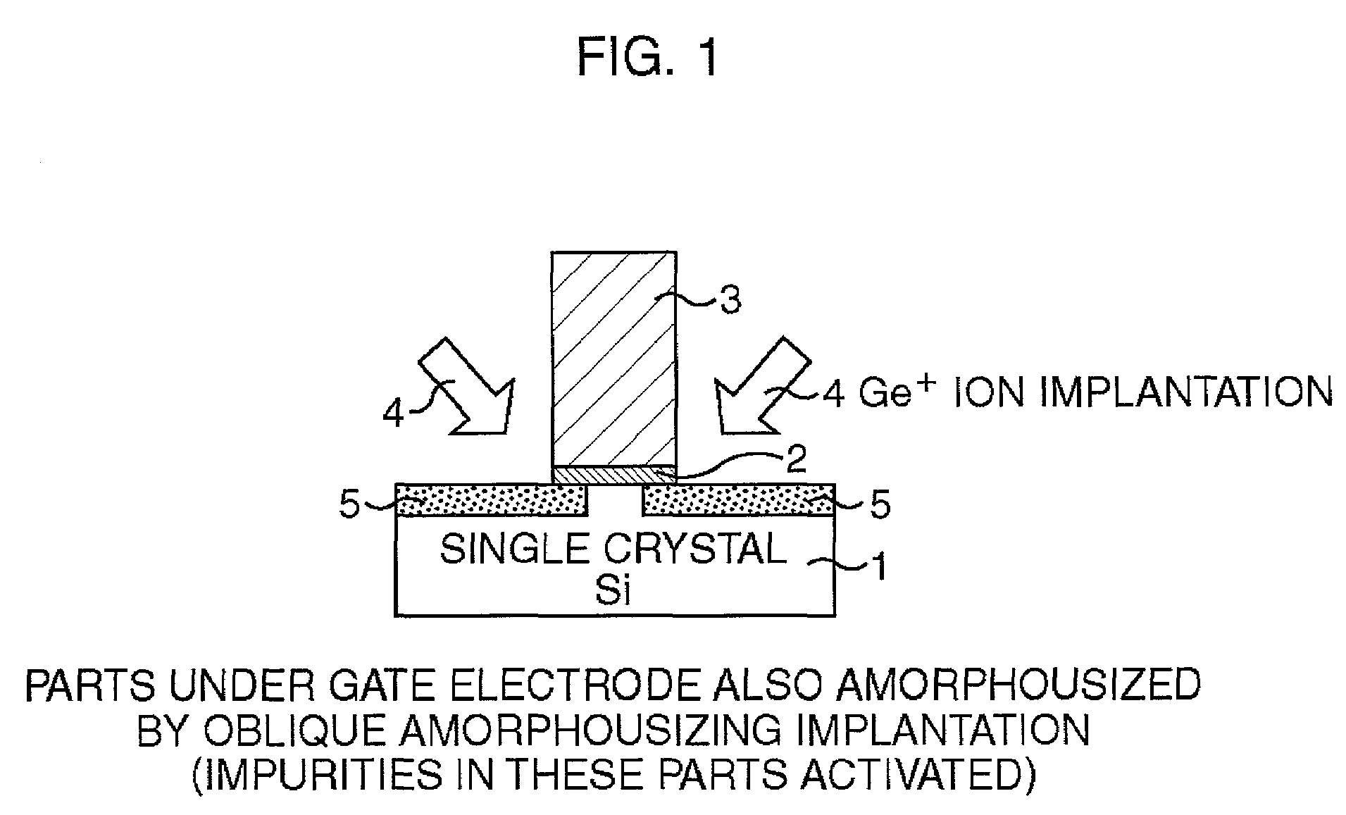
[0039]First, the first embodiment is explained in order of step using FIGS. 5A to 5E and FIGS. 6A to 6C.

(1) From Element Isolation to Gate Electrode Formation (FIG. 5A)

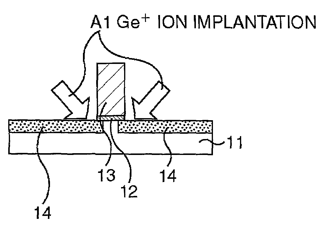
[0040]First, on a semiconductor substrate 11 made of single crystal Si, normal process of manufacturing a MOS transistor is executed which includes the formation of a not shown element isolation structure for defining an element region (a field oxide film by the LOCOS method, a local insulating film by the STI method and so on), the formation of a well structure by ion implantation of impurities, ion implantation for controlling the threshold value and so on.

[0041]Then, a gate insulating film 12 is formed on the defined element region of the semiconductor substrate 11. This gate insulating film is of one type selected from among a silicon oxide film, a silicon nitride film, a silicon oxynitride film and a metal oxide film having a dielectric constant higher than that of the silicon oxide film, or of a film having a la...

second embodiment

[0057]Next, the second embodiment is explained in order of step using FIGS. 7A to 7D.

(1) From Element Isolation to Gate Electrode Formation (FIG. 7A)

[0058]First, on a semiconductor substrate 11 made of single crystal Si, normal process of manufacturing a MOS transistor is executed which includes the formation of a not shown element isolation structure for defining an element region (a field oxide film by the LOCOS method, a local insulating film by the STI method and so on), the formation of a well structure by ion implantation of impurities, ion implantation for controlling the threshold value and so on.

[0059]Then, a gate insulating film 12 is formed on the defined element region of the semiconductor substrate 11. This gate insulating film is of one type selected from among a silicon oxide film, a silicon nitride film, a silicon oxynitride film and a metal oxide film having a dielectric constant higher than that of the silicon oxide film, or of a film having a laminated structure t...

third embodiment

[0069]Next, the third embodiment is explained in order of step using FIGS. 8A to 8D.

(1) From Element Isolation to Gate Electrode Formation (FIG. 8A)

[0070]First, on a semiconductor substrate 11 made of single crystal Si, normal process of manufacturing a MOS transistor is executed which includes the formation of a not shown element isolation structure for defining an element region (a field oxide film by the LOCOS method, a local insulating film by the STI method and so on), the formation of a well structure by ion implantation of impurities, ion implantation for controlling the threshold value and so on.

[0071]Then, a gate insulating film 12 is formed on the defined element region of the semiconductor substrate 11. This gate insulating film is of one type selected from among a silicon oxide film, a silicon nitride film, a silicon oxynitride film and a metal oxide film having a dielectric constant higher than that of the silicon oxide film, or of a film having a laminated structure th...


PUM


Abstract

To make it possible to obtain a sharp impurity profile without presenting a disadvantage such as an increase in parasitic resistance or the like using a laser annealing method to thereby meet sufficiently the requirements for making a semiconductor element finer and more highly integrated. A gate electrode is pattern formed above a semiconductor substrate made of n-type silicon single crystal through a gate insulating film. Thereafter, atoms, Ge+ here, having properties just enough to amorphize single crystal Si are ion implanted (shown by arrows) from oblique directions to the Si surface of the substrate with the gate electrode as a mask to melt and re-crystallize the single crystal Si so as to form amorphous regions which seep into the substrate under the gate electrode. Thereafter B+ ions are implanted into the amorphous regions and laser irradiation is executed thereon.

Description

CROSS-REFERENCE TO RELATED APPLICATIONS[0001]This application is based upon and claims priority of Japanese Patent Application Nos. 2001-059060, filed on Mar. 2, 2001 and 2002-024468, filed on Jan. 31, 2002, the contents being incorporated herein by reference.BACKGROUND OF THE INVENTION[0002]1. Field of the Invention[0003]The present invention relates to a method of manufacturing a semiconductor device and, more specifically, is preferably applied to the formation of a source and a drain in a MOS transistor of a generation having a gate length of less than 0.1 μm.[0004]2. Description of the Related Art[0005]In recent years, the laser annealing technique is expected as thermal process of the next generation, replacing rapid lamp heating. This technique, nonequilibrium thermal process which is a melting and re-crystallization process in a very short period of time of several nanoseconds, has advantages in its capability of obtaining high electrical activity exceeding the solubility li...

Claims


Application Information

Patent Timeline
Patent Type & Authority Patents(United States)
IPC IPC(8): H01L21/336H01L29/78H01L21/265H01L21/268H01L21/8234H01L21/8238H01L27/088H01L27/092
CPCH01L21/26506H01L21/26513H01L21/26586H01L21/268H01L21/823807H01L21/823814H01L29/6659
Inventor YAMAMOTO, TOMONARI
Owner FUJITSU SEMICON LTD
Why Eureka
Try Eureka