
Power bipolar transistor and manufacture method thereof
A bipolar transistor and power technology, which is applied in the manufacture of transistors, semiconductor/solid-state devices, electrical components, etc., can solve the problems of power bipolar transistors, such as power consumption, high hazard, and increase of parasitic resistance of the base region, and achieves The effect of alleviating the current edge-setting effect in the emitter region and improving the secondary breakdown power capacity
- Summary
- Abstract
- Description
- Claims
- Application Information
AI Technical Summary
Problems solved by technology
Method used
Image

Examples
Embodiment Construction
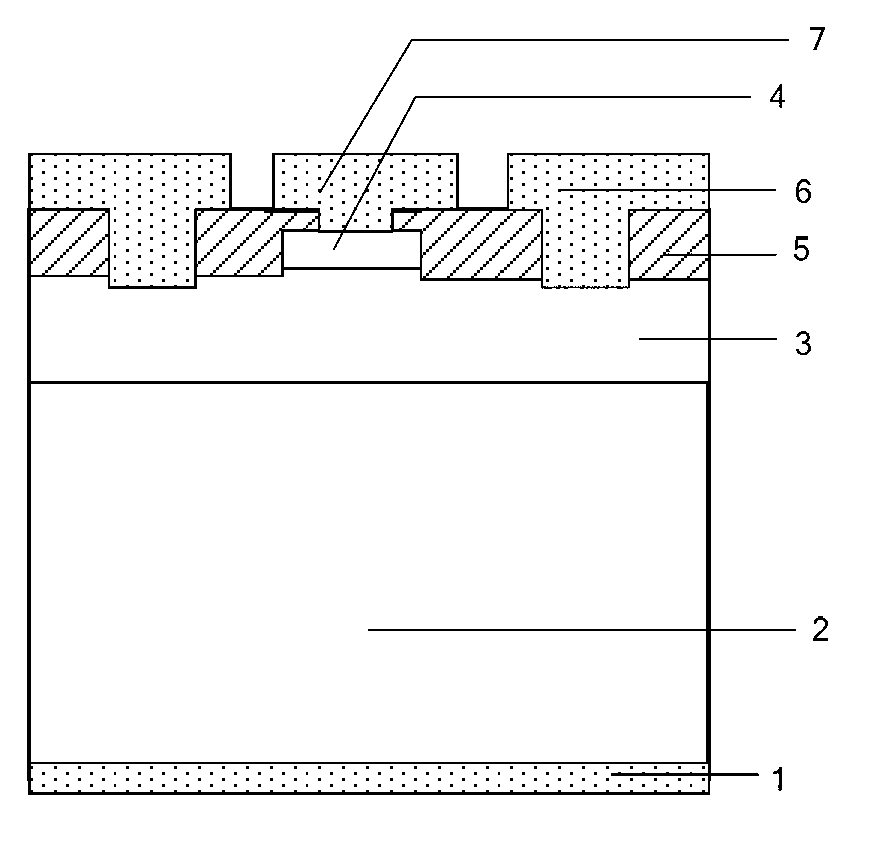
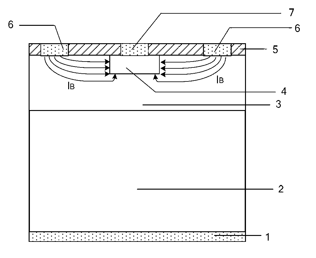
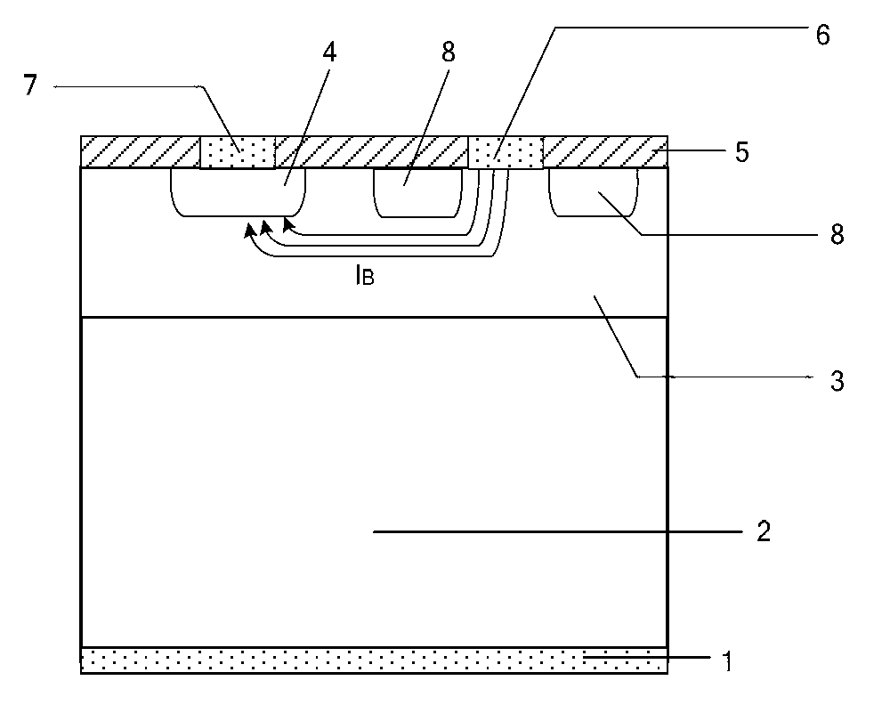
[0029] A power bipolar transistor such as figure 1 As shown, it includes from bottom to top: metal electrode 1 in the collector region, collector region 2 made of heavily doped semiconductor material of the first conductivity type, base region 3 made of semiconductor material of the second conductivity type; base region 3 There are metal electrodes 6 in the base area and an emission area 4 made of the first conductivity type semiconductor material which are in contact with the surface of the base area 3; above the emission area 4 are metal electrodes 7 in contact with the surface of the emission area 4; An isolation medium 5 is filled between the sidewall of the emitter region 4 and the metal electrode 6 of the base region, and between the metal electrode 6 of the base region and the metal electrode 7 of the emitter region.
[0030] A preparation method of a power bipolar transistor, as shown in the figure Figure 5-a — Figure 5-f shown, including the following steps:
[...
PUM
 Abstract
Description
Claims
Application Information