Data reception device

a data reception and data technology, applied in the field of data reception devices, can solve the problems of increasing cost, affecting the operation speed of liquid crystal panel modules, and affecting the operation speed of the system, so as to achieve high speed operation, low power consumption, and low cost

Active Publication Date: 2018-06-26
CEREBREX ZHUHAI CO LTD
View PDF18 Cites 6 Cited by
  • Summary
  • Abstract
  • Description
  • Claims
  • Application Information

AI Technical Summary

Benefits of technology

[0012]Meanwhile, a so-called system driver in which a timing controller and a source driver are configured as one chip as illustrated in in FIG. 17 is implemented in some tablet PCs and the like. When the system driver is implemented, the number of parts is reduced so that the cost can be reduced. Furthermore, since there is no interface between the timing controller and the source driver, the power consumption can be also reduced. However, the system driver is mounted on a glass of a liquid crystal panel similarly to the source driver. In addition, drawing data is directly input to the system driver from the CPU or the GPU via the eDP interface or the mipi interface. However, a wiring on the glass has a high parasitic resistance, and thus, it is difficult to improve an operating frequency in the case of a gigabit-class serial high-speed interface such as the eDP and the mipi, which makes the increase of resolution difficult. In addition, a configuration in which the system driver of the panel is driven directly from the CPU or the GPU is also conceivable. Even in this case, however, it is difficult to achieve high resolution due to noise on the transmission line of the cable and fluctuations in power supply.
[0032]The present invention can dynamically control the gain value of the equalizer circuit in a display module of a mobile device, such as a laptop PC and a tablet terminal, and the like. For example, it is possible to realize the high-speed operation of the single-chip system driver even in the operating environment of being mounted on the glass and having the high parasitic resistance, and thus, it is possible to achieve both the low power consumption and low cost of the liquid crystal panel module and the like.

Problems solved by technology

Meanwhile, a data processing amount and an operating frequency have steadily increased along with improvement of resolution of a panel and improvement of image quality of a display, and the reduction of the power consumption and the cost reduction have become major problems which conflict thereto.
The data processing amount and the frequency have steadily increased along with the improvement of resolution of the panel even in the tablet terminal, and the power consumption becomes a major problem.
In a recent high-resolution display panel, however, the mini-LVDS has been hardly used because a screw, which is a gap in timing on a transmission path generated when a clock line as a reference signal and a transmission data line are separated, becomes a problem.
Furthermore, a flexible printed cable (FPC) for connection between the timing controller and the source driver is required as many as the number of source drivers so that the number of parts has increased along with the increase of resolution of the panel, which causes an increase in cost.
Furthermore, it is absolutely necessary to provide the interface between the timing controller and the source driver, and thus, power consumption of the interface is required.
Based on such a background, it has been difficult to reduce the cost and the power consumption.
However, a wiring on the glass has a high parasitic resistance, and thus, it is difficult to improve an operating frequency in the case of a gigabit-class serial high-speed interface such as the eDP and the mipi, which makes the increase of resolution difficult.
Even in this case, however, it is difficult to achieve high resolution due to noise on the transmission line of the cable and fluctuations in power supply.
However, in the case of the conventional analog front-end circuit configuration, the operation is performed at operation speed in a range between 1.62 Gbps and 8.1 Gbps in the high-speed serial interface such as the eDP, and thus, signal quality greatly deteriorates due to a glass wiring resistance.
In addition, it is difficult for the equalizer circuit and the CDR circuit to properly operate in environment where a large power supply drop is generated even in a power supply and a ground line due to the parasitic resistance.
A DC level of a signal component is close to a high level after “1” continues for a certain period of time, and thus, there is a problem that it is difficult for the subsequent “0” data to be inverted to a low level.
On the contrary, the DC level is close to the low level after “0” continues for a certain period, and thus, there is a problem that it is difficult for the subsequent “1” data to be inverted to the high level.
Further, as illustrated in FIG. 21, a waveform of output from the equalizer circuit is disturbed regardless of whether the gain value of the equalizer circuit is too strong or weak, and it is difficult to correctly perform recovery of the signal in the CDR circuit at the subsequent stage.
For example, if the gain value of the equalizer circuit is too weak, the output waveform thereof has a time axis direction of the signal shorter than the original time, which makes it impossible to correctly determine the logic level.
On the other hand, if the gain value of the equalizer circuit is too strong, the output waveform thereof has the time axis direction of the signal longer than the original time, which makes it impossible to correctly determine the logic level.
However, it is difficult for a gain setting value of the equalizer circuit to dynamically follow an environmental variation factor that dynamically changes due to such ambient environment in the conventional technology, and thus, there is a limitation in increasing a bit rate.
As described above, the output waveform of the equalizer circuit is disturbed regardless of whether the gain value of the equalizer circuit is too strong or weak, and it is difficult to correctly recover the signal by the CDR circuit at the subsequent stage.
Conventionally, however, it is difficult for the gain setting value of the equalizer circuit to dynamically follow such a dynamically changing environmental variation factor, and thus, there is a limitation in increasing the bit rate.
Influence that the delay (timing skew) between the data signal and the clock signal gives on a timing budget becomes more serious as the operation speed becomes faster, which becomes one factor that hinders the increase in speed.

Method used


Image

  • Data reception device
  • Data reception device
  • Data reception device

Examples


first embodiment

[0055][First Embodiment of Present Invention]

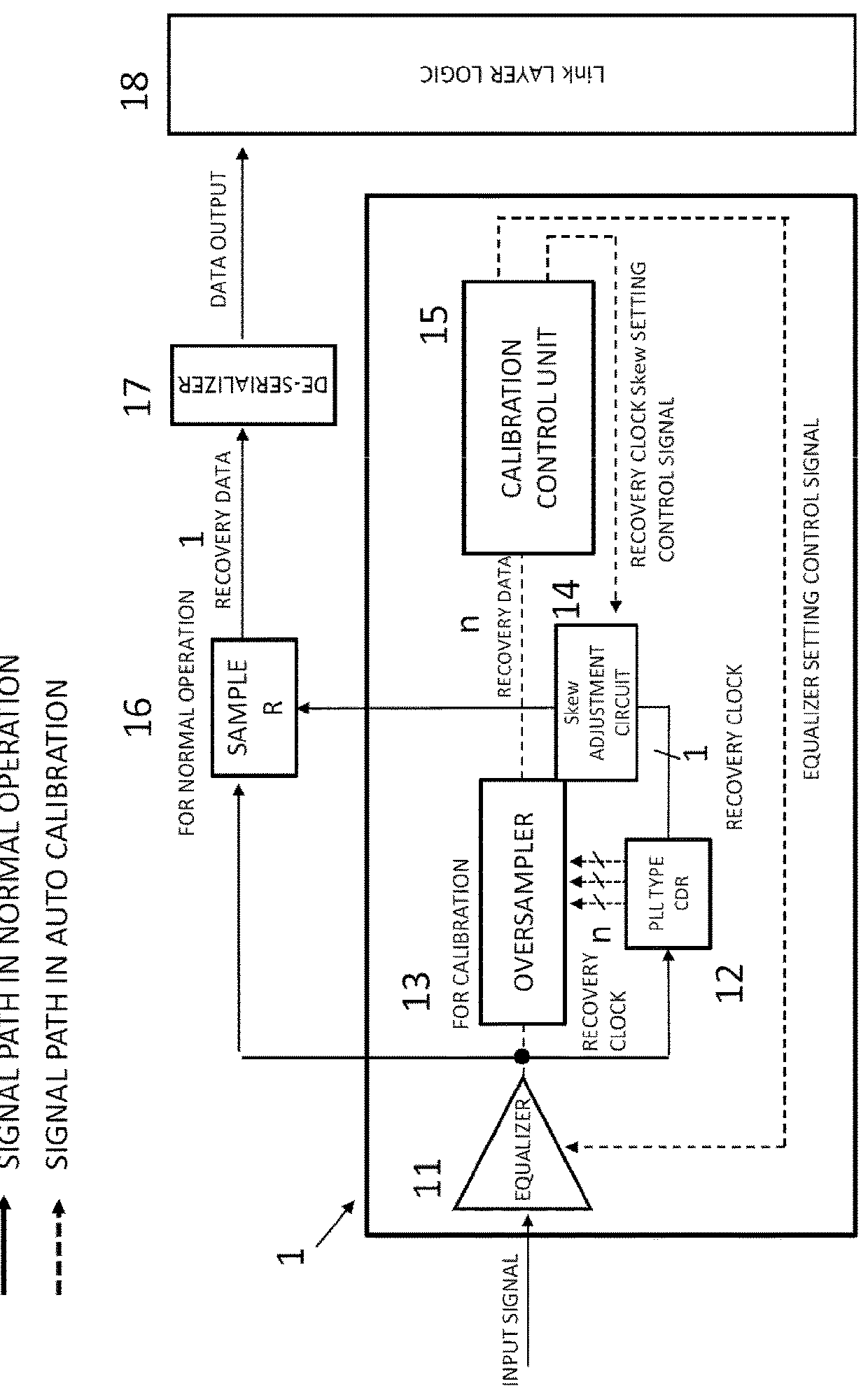
[0056]A first embodiment of the present invention will be described. FIG. 1 is a block diagram for describing an overall configuration of a data receiving circuit 1 according to the present invention. Here, a basic configuration of the data receiving circuit 1 will be described with reference to FIG. 1.

[0057]The data receiving circuit 1 is a circuit incorporated in a timing controller in, for example, a laptop PC or a tablet PC and receives drawing data transmitted from a processor such as a CPU and a GPU. The timing controller is a large-scale integration (LSI) that generates various timing signals so that drawing data transmitted from the processor such as the CPU and the GPU matches a timing of a liquid crystal panel. The interface between the processor and the timing controller conforms to, for example, an eDP standard of VESA. That is, the timing controller receives the drawing data from the processor through a Main-Link (main signal...

second embodiment

[0080][Second Embodiment of Present Invention]

[0081]A second embodiment of the present invention will be described. The second embodiment of the present invention is given as follows. In the first embodiment described above, the gain level of the equalizer circuit can be optimally set in the link training sequence at the time of starting the power supply. However, a power supply level of the IC fluctuates depending on an operation state, and temperature also fluctuates even after the link training is completed and the operation is shifted to the normal operation. Since such fluctuations in the power supply level and temperature affect characteristics of the equalizer circuit as described above, it is desirable to periodically review (calibrate) the optimum value even after shifting to the normal operation. As described above, the contact resistance of the IC mounted on the glass changes with time, and the resistance value may increase in some cases. In view of these phenomena, there...

third embodiment

[0083][Third Embodiment of Present Invention]

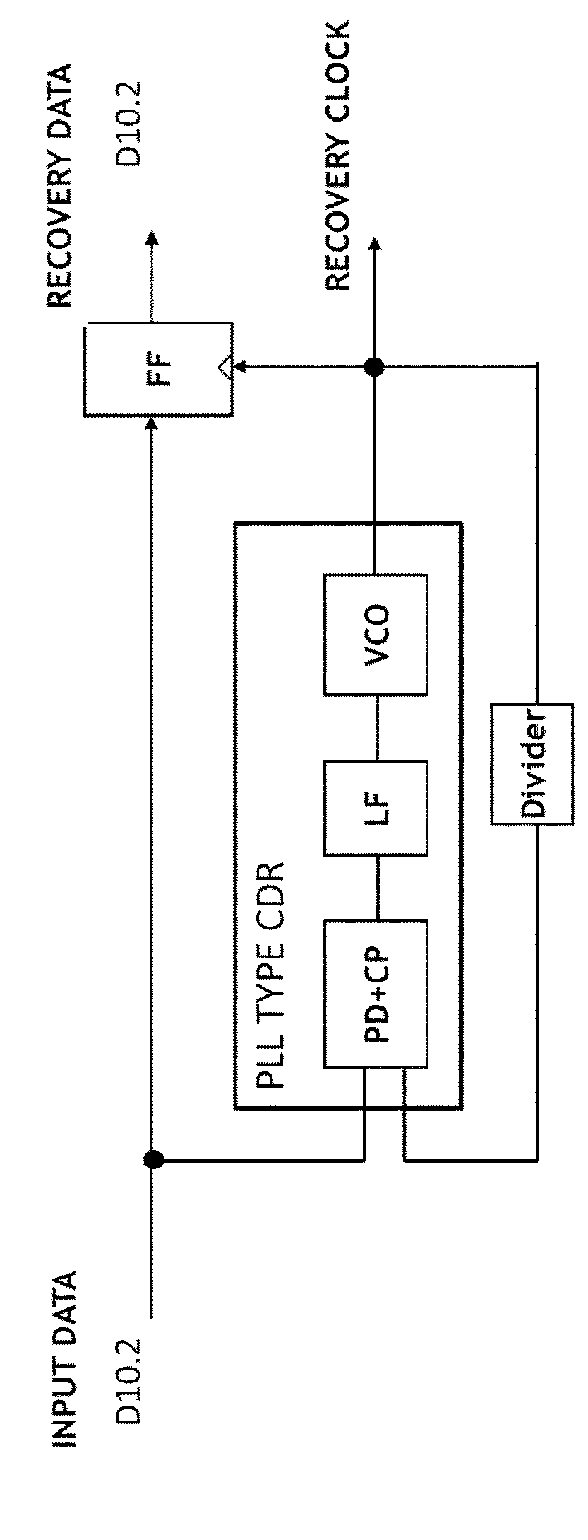
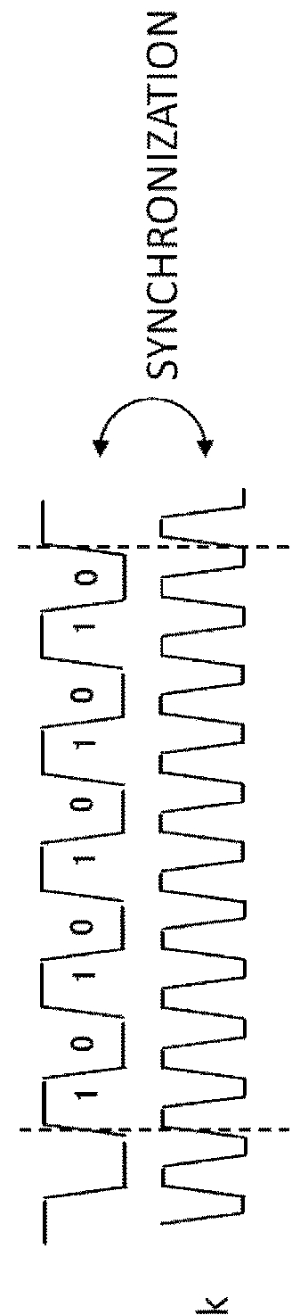
[0084]A third embodiment of the present invention will be described. The third embodiment of the present invention is given as follows. As described above, the clock is superimposed on the data line in the high-speed serial interface such as the eDP, and it is necessary to extract the clock synchronized with the data from the serial data input. Therefore, the CDR circuit is the circuit which generates the clock signal synchronized in timing with the data from the serial data input. The CDR circuit is generally configured using the PLL. Although the sampler during the normal operation samples a data signal as output from the equalizer circuit and a clock signal as output from the PLL, a delay from the equalizer circuit to the sampler varies depending on the power supply fluctuations, the temperature fluctuations, and the semiconductor manufacturing variation no matter how carefully a layout is designed. Influence that the delay (timing ske...


PUM


Abstract

A data reception device includes: an equalizer circuit that shapes a waveform of an input signal according to a set gain value; a CDR circuit which recovers a plurality of clock signals having different phases in one cycle from the input signal after being subjected to the waveform shaping performed by the equalizer circuit; an oversampler which performs sampling of the waveform-shaped input signal in synchronization with the plurality of clock signals and recovers a plurality of input data from the waveform-shaped input signal; and a calibration control unit which determines whether the oversampler correctly recovers the input data based on a result of the sampling performed by the oversampler, and generates a control signal to set the gain value of the equalizer circuit based on a determination result when it is determined that the input data is not correctly recovered.

Description

BACKGROUND[0001]Technical Field[0002]The present invention relates to a data reception device in an interface for transmitting image data to a liquid crystal panel module at high speed.[0003]Related Art[0004]In a market for mobile devices such as laptop PC and tablet PC, there always is a request for reduction in power consumption and cost. Meanwhile, a data processing amount and an operating frequency have steadily increased along with improvement of resolution of a panel and improvement of image quality of a display, and the reduction of the power consumption and the cost reduction have become major problems which conflict thereto.[0005]As flow of drawing data to the panel in the laptop PC or the tablet PC, it is configured to use a processor such as a central processing unit (CPU) and a graphics processing unit (GPU) that are in charge of calculation of the drawing data itself, various calculation processing and graphics processing, a timing controller (TCON) that performs timing...

Claims


Application Information

Patent Timeline
Patent Type & Authority Patents(United States)
IPC IPC(8): H04L25/03H04L7/00
CPCH04L25/03885H04L7/0079H04L7/0016
Inventor SUZUKI, SHINYAKONISHI, KENZONAGANO, HIDEOKATO, MASAHIRO
Owner CEREBREX ZHUHAI CO LTD
Why Eureka
Try Eureka