LDMOS (laterally diffused metal oxide semiconductor) device and manufacturing method thereof

A device and drift region technology, applied in the manufacture of LDMOS devices, in the field of lateral field effect transistors (LDMOS devices, it can solve the limitations of the increase in the doping concentration of the drift region, the reduction in length, the large and short channel effects, and the increase in process costs, etc. problem, to achieve high breakdown voltage, reduce parasitic resistance, reduce the effect of on-resistance

Active Publication Date: 2015-04-15
SHANGHAI HUAHONG GRACE SEMICON MFG CORP
View PDF2 Cites 6 Cited by
  • Summary
  • Abstract
  • Description
  • Claims
  • Application Information

AI Technical Summary

Problems solved by technology

However, LDMOS must meet the requirements of the breakdown voltage, and the increase of the doping concentration and the reduction of the length of the drift region are subject to certain restrictions.
The increase in the thickness of the drift region can only be formed by high-energy ion implantation and long-time well pushing in the non-epitaxial process, but this will cause excessive lateral diffusion and cause excessive short-channel effects
Epitaxial LDMOS can form a thick drift region, but the process cost increases

Method used


Image

  • LDMOS (laterally diffused metal oxide semiconductor) device and manufacturing method thereof
  • LDMOS (laterally diffused metal oxide semiconductor) device and manufacturing method thereof
  • LDMOS (laterally diffused metal oxide semiconductor) device and manufacturing method thereof

Examples


Embodiment Construction

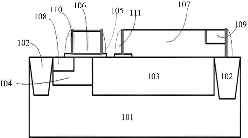
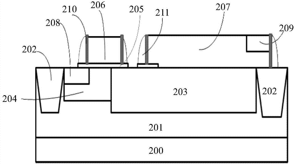
[0046] The LDMOS device of the embodiment of the present invention includes:

[0047] A silicon substrate doped with a first conductivity type.

[0048] The first drift region is composed of a second conductivity type ion implantation region formed in a selected region of the silicon substrate.

[0049] The channel region is composed of a well region of the first conductivity type formed in a selected region of the silicon substrate, and the first side of the first drift region is in contact with the channel region in the lateral direction.

[0050] A polysilicon gate formed above the channel region, a gate dielectric layer is isolated between the polysilicon gate and the silicon substrate, the polysilicon gate covers part of the channel region and extends above the first drift region , the surface of the channel region covered by the polysilicon gate is used to form a channel.

[0051] A source region is composed of a heavily doped region of the second conductivity type for...


PUM

PropertyMeasurementUnit
Thicknessaaaaaaaaaa

Abstract

The invention discloses an LDMOS (laterally diffused metal oxide semiconductor) device and a manufacturing method thereof. A drift region of the LDMOS device comprises a first drift region and a second drift region; the first drift region is formed by an ion implantation region formed in a selected area of a silicon substrate; the second drift region is formed by doped polysilicon formed on the surface of the silicon substrate; the second drift region is overlapped on the first drift region, and a drain region is formed in the second drift region. Owing to arrangement of the second drift region, thickness of the whole drift region is increased, and accordingly parasitic resistance of the whole drift region is reduced while effectiveness in increase of linear current of the device and reduction of on resistance of the device can be achieved. In addition, the LDMOS device is capable of keeping high breakdown voltage and is low in process cost.

Description

technical field [0001] The invention relates to the field of semiconductor integrated circuit manufacturing, in particular to a lateral field effect transistor (LDMOS device; the invention also relates to a method for manufacturing the LDMOS device. Background technique [0002] Lateral Field Effect Transistor (LDMOS) is a commonly used semiconductor high-voltage device, which is widely used in power management, LCD and LED driving, ESD protection and other fields. There are usually two application methods: analog application and switch application. When LDMOS is used as a switch, the device needs to have a very low on-resistance (source-drain resistance of the device in the linear region) to reduce switching power consumption. In LDMOS, the channel length is much smaller than the length of the drift region, and the on-resistance of the device is dominated by the resistance of the drift region. Therefore, in switching LDMOS, it is necessary to increase the doping concentrat...

Claims


Application Information

Patent Timeline
IPC IPC(8): H01L29/78H01L29/06H01L21/336H01L21/265
CPCH01L21/324H01L29/0684H01L29/66681H01L29/7816H01L29/0847H01L29/66659H01L29/7835
Inventor 钱文生
Owner SHANGHAI HUAHONG GRACE SEMICON MFG CORP
Why Eureka
Try Eureka