

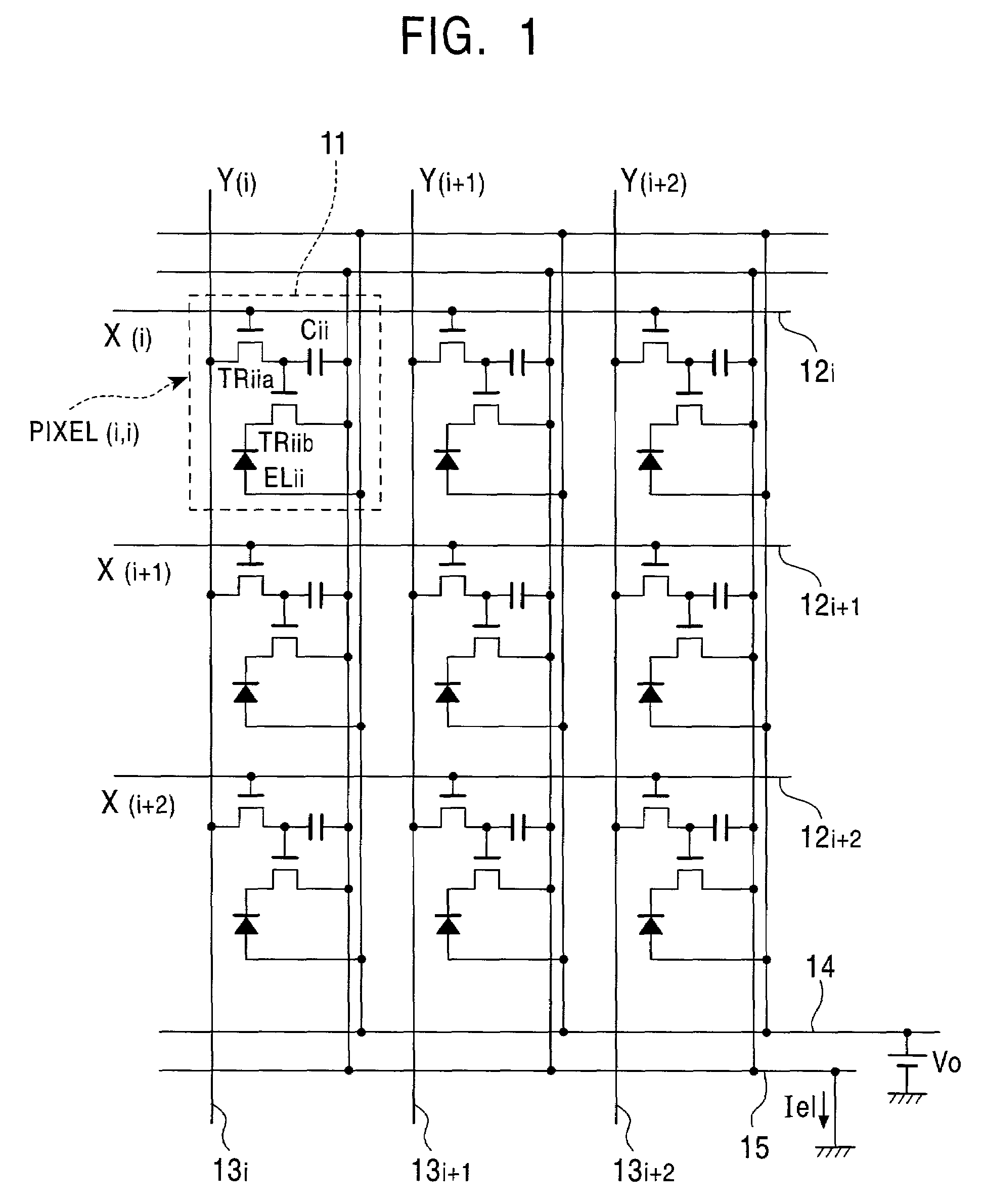
Active matrix display
a technology of active matrix and display, applied in the field of active matrix display, can solve the problems of inevitable roughness or step of a few micrometers, and achieve the effects of reducing the roughness of the circuitry layer, improving the reliability improving the flatness of the lower electrode of the luminescent device, which overlies the circuitry layer
- Summary
- Abstract
- Description
- Claims
- Application Information
AI Technical Summary
Benefits of technology
Problems solved by technology
Method used
Image

Examples
first embodiment
[0035]FIG. 4 is a plane view showing a combination of the arrangements of organic EL devices and pixel circuits according to a first embodiment. The organic EL devices for emitting RGB lights are arrayed in a stripe arrangement in the device layer 38, as shown in (a) of FIG. 4. The areas within broken lines shown in (a) of FIG. 4 are emitting areas for pixels. The pixel circuits are also arrayed in a stripe arrangement in the circuitry layer 32, as shown in (b) of FIG. 4
[0036]Since all the pixel circuits in the circuitry layer 32 have the same structure, the contacts 39, each connecting an organic EL device with a pixel circuit, are regularly arrayed. For example, here, the contacts 39 are arrayed in a single dimension in every row of the arrangement of the pixel circuits, positioned at the center of pixel circuits.
[0037]In this instance, if the device layer 38 is deposited on the circuitry layer 32 such that each organic EL device opposes a pixel circuit, the contacts 39 cannot be ...
second embodiment
[0039]FIG. 5 is a plane view showing a combination of the arrangements of organic EL devices and pixel circuits according to a second embodiment. In the second embodiment, the organic EL devices and the pixel circuits are arrayed in a stripe arrangement in the device layer 38 and the circuitry layer 32, respectively, in the same manner as the first embodiment.
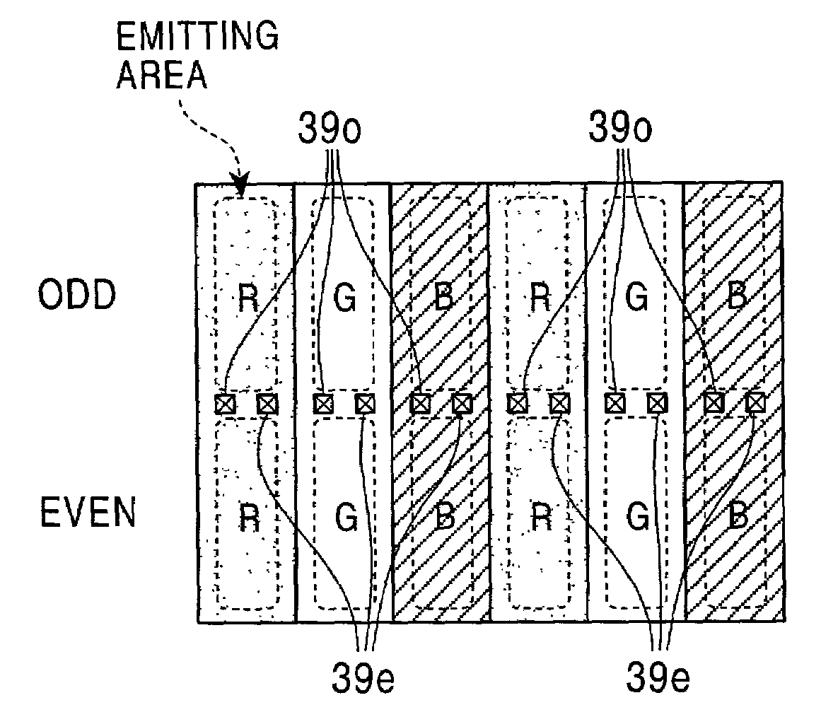
[0040]However, the device layer 38 overlies the circuitry layer 32 such that each organic EL device opposes a pixel circuit instead of being offset. The pixel circuits are, therefore, prepared in the circuitry layer 32 such that the contacts 39 will be positioned out of the emitting areas of the pixel units in the device layer 38.
[0041]Preferably, the contacts 39 for the pixel units in two adjacent rows in the pixel arrangement, that is, the contacts 39o for an odd row and the contacts 39e for an even row are arrayed in a single dimension between the two rows. Thus, the contacts 39 are positioned out of the emitting areas of th...
third embodiment
[0043]FIG. 6 is a plane view showing a combination of the arrangements of organic EL devices and pixel circuits according to a third embodiment. The third embodiment, while organic EL devices for emitting RGB lights are arrayed in a delta arrangement in the device layer 38, the pixel circuits are arrayed in a stripe arrangement in the circuitry layer 32.
[0044]In the third embodiment as well as in the second embodiment, the device layer 38 overlies the circuitry layer 32 such that each organic EL device opposes a pixel circuit, and the pixel circuits are prepared in the circuitry layer 32 such that the contacts 39 will be positioned out of the emitting areas of the pixel units in the device layer 38.
[0045]Preferably, the contacts 39 for the pixel units in two adjacent rows in the pixel arrangement, that is, the contacts 39o and 39e are arrayed in a single dimension between the two rows, as shown in FIG. 6. Thus, the contacts 39 are positioned out of the emitting areas to minimize the...
PUM
 Abstract
Description
Claims
Application Information