
Method for reducing surface roughness while producing a high quality useful layer

a technology of useful layer and surface roughness, which is applied in the manufacturing of semiconductor/solid-state devices, basic electric elements, electric devices, etc., can solve the problems of compromising the uniformity of the free surface of the thin layer, cold working defects, chemical-mechanical polishing causes defects, etc., and achieves the effect of minimizing low-frequency roughness, minimizing high-frequency roughness of the surface, and high quality

Inactive Publication Date: 2015-08-06
SOITEC SA
View PDF3 Cites 0 Cited by
  • Summary
  • Abstract
  • Description
  • Claims
  • Application Information

AI Technical Summary

Benefits of technology

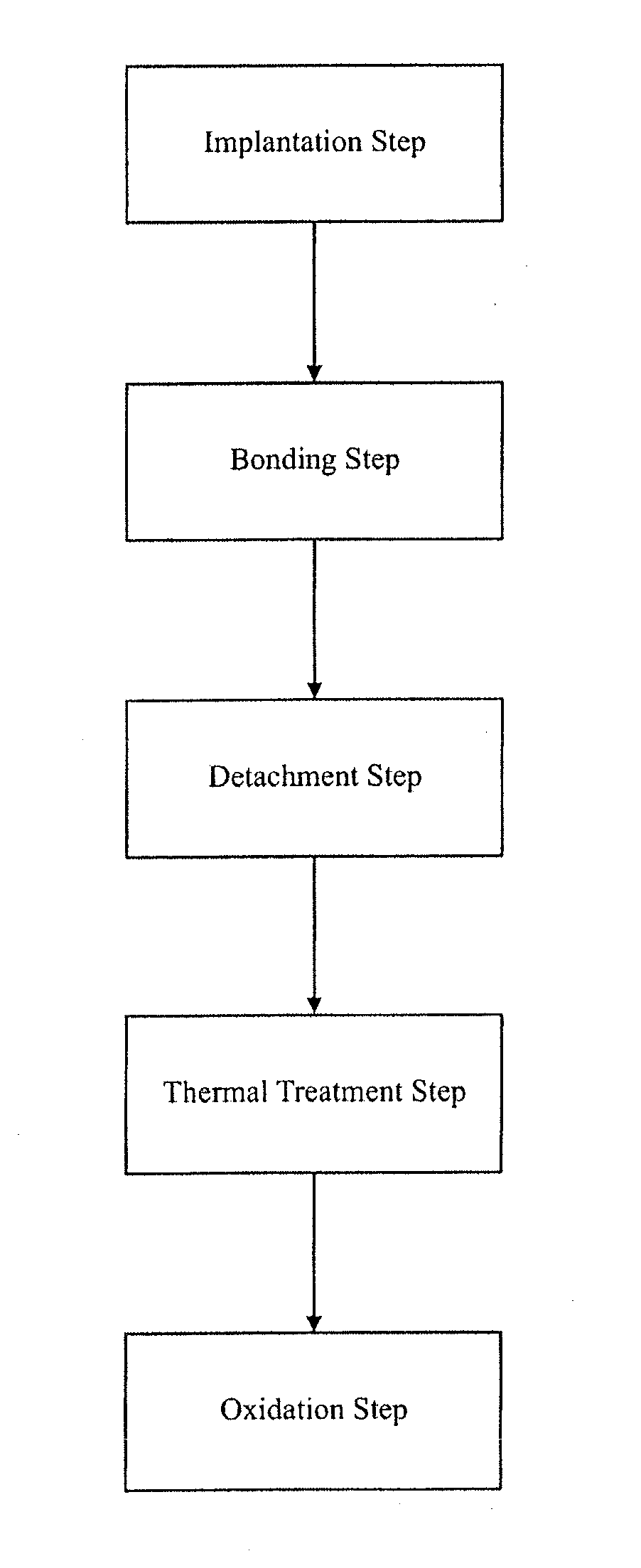
The patent is about a new method for making a high-quality layer of semiconductor material on a substrate. The method involves implanting two different atomic species into a donor substrate to create a weakened zone and define a useful layer. The surface of the useful layer is then heat-treated to reduce roughness and make it ready for further processing without needing to use chemical-mechanical polishing. This new method improves the quality of the thin useful layer by decreasing surface roughness, improving uniformity, and reducing defects. It effectively treats both low-frequency and high-frequency structural roughness without needing to use CMP polishing.

Problems solved by technology

However, chemical-mechanical polishing causes defects (for example, cold working defects) in the thin layer.
In addition, it compromises the uniformity of the free surface of the thin layer (in particular uniformity according to very low frequencies).
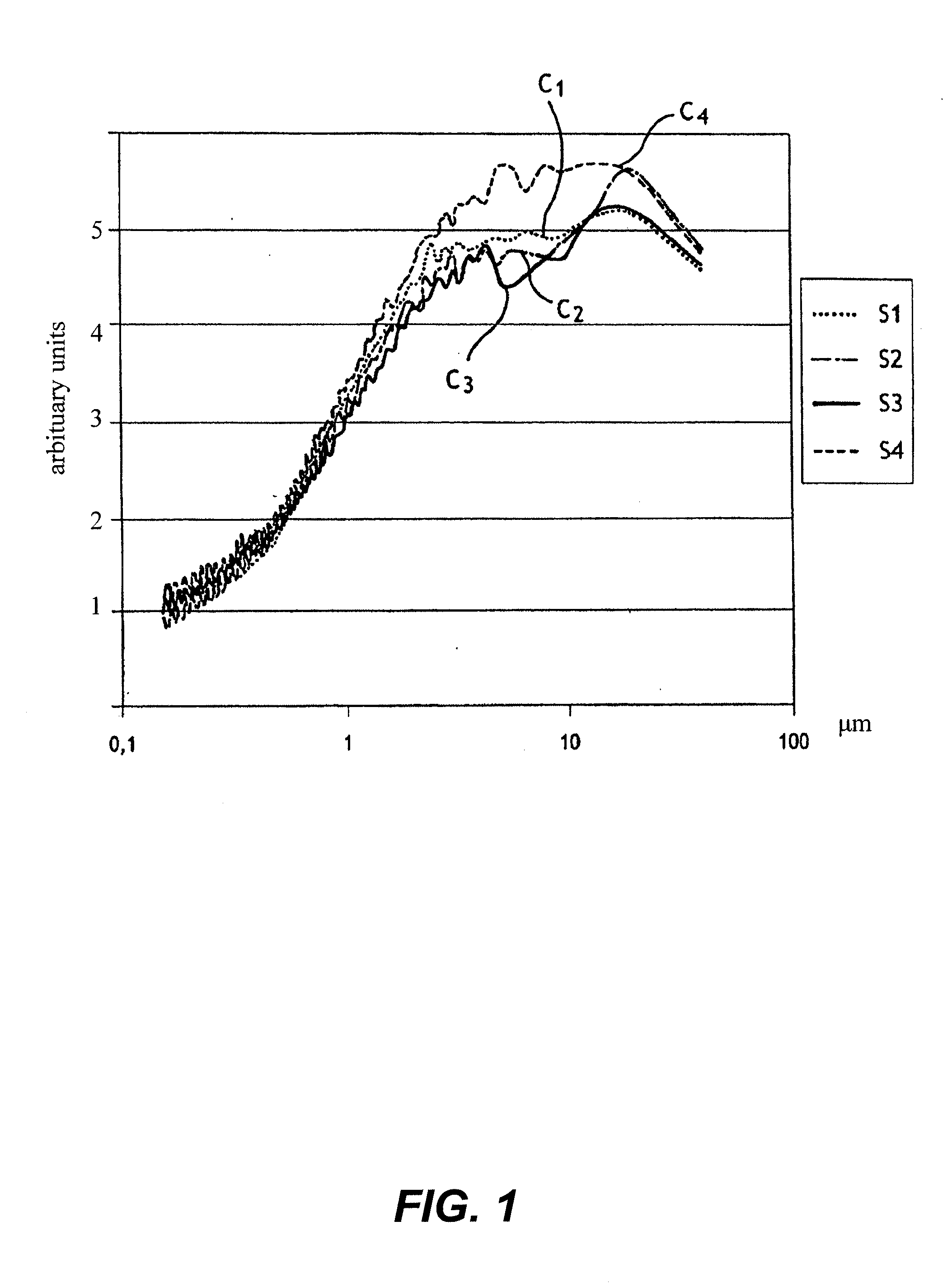
But this treatment does not totally eliminate the lowest-frequency roughness (5 to 10 micrometers).
In the case of such treatment, annealing in a reducing atmosphere is beneficial for smoothing the high-frequencies roughness (a spatial period of less than 3 Angstroms), but is less efficient for reducing waviness, which are the low-frequency roughness parameters.
Therefore, the known processes for improving the quality of the thin layer of a structure of the type described above include limitations and / or drawbacks.

Method used


Image

  • Method for reducing surface roughness while producing a high quality useful layer
  • Method for reducing surface roughness while producing a high quality useful layer
  • Method for reducing surface roughness while producing a high quality useful layer

Examples


Embodiment Construction

[0026]The present process relates to the production of structures that include a thin layer of semiconductor material on a support substrate, wherein the thin layer is by detachment at the level of a donor substrate that has a weakened zone created by implantation of species. The structure can be, in general, any type of structure that includes a thin layer of a semiconductor material on a surface exposed to the external environment (a free surface). Such a thin layer of semiconductor material can be, for example, silicon Si, silicon carbide SiC, germanium Ge, silicon-germanium SiGe, gallium arsenic AsGa, etc. Further, a support substrate can be made of silicon Si, quartz, and the like. A layer of oxide can also be inserted between the support substrate and the thin layer, such that the structure that is formed is a semiconductor-on-insulator structure (such as a SeOI structure), and in particular a silicon-on-insulator (SOI) structure, for example).

[0027]The invention can advantage...


PUM

PropertyMeasurementUnit
temperatureaaaaaaaaaa
roughnessaaaaaaaaaa

Abstract

A method for producing a high quality useful layer of semiconductor material on a substrate. The method includes implanting at least two different atomic species into a face of a donor substrate to a controlled mean implantation depth to form a weakened zone therein and to define a useful layer. The implanting step is conducted to minimize low-frequency roughness at the weakened zone. Next, the method includes bonding a support substrate to the face of the donor substrate, and detaching the useful layer from the donor substrate along the weakened zone. A structure is thus formed that includes the useful layer on the support substrate with the useful layer presenting a surface for further processing. The technique also includes thermally treating the structure to minimize high-frequency roughness of the surface of the useful layer. The result is a surface having sufficient smoothness so that chemical-mechanical polishing (CMP) is not needed.

Description

CROSS-REFERENCE TO RELATED APPLICATIONS[0001]This application is a continuation of U.S. patent application Ser. No. 11 / 446,357, filed Jun. 5, 2006, pending, which is a continuation of U.S. patent application Ser. No. 10 / 691,403, filed Oct. 21, 2003, now U.S. Pat. No. 7,081,399, issued Jul. 25, 2006, which also claims the benefit of the filing date of French Patent Application Serial No. FR0309304, filed Jul. 29, 2003, the entire contents of each of which are incorporated herein by reference thereto.BACKGROUND ART[0002]The present invention generally relates to a method for producing a high quality useful layer of semiconductor material on a substrate. In particular, the method includes implanting at least two different atomic species into a face of a donor substrate to a controlled mean implantation depth to form a weakened zone therein and to define a useful layer. The implanting step is conducted to minimize low-frequency roughness at the weakened zone. Next, a support substrate i...

Claims


Application Information

Patent Timeline
Patent Type & Authority Applications(United States)
IPC IPC(8): H01L21/762H01L21/324
CPCH01L21/324H01L21/76254H01L21/762
Inventor MALEVILLE, CHRISTOPHENEYRET, ERICBEN MOHAMED, NADIA
Owner SOITEC SA
Learn More