Pad layouts of a printed circuit board

a printed circuit board and layout technology, applied in the field of layouts of printed circuit boards, can solve the problems of limited space on the printed circuit board, reduced available space for electronic components, and only capable of receiving a certain number of sm

Inactive Publication Date: 2008-11-04
HONG FU JIN PRECISION IND (SHENZHEN) CO LTD +1
View PDF22 Cites 5 Cited by
  • Summary
  • Abstract
  • Description
  • Claims
  • Application Information

AI Technical Summary

Benefits of technology

[0014]By use of above described shapes, the surface area of the pads are minimized thereby reducing incidents of floating of small sized components, and reducing cost by minimizing materials used in manufacturing the pads. Further, in the design layout process of a PCB, by using pads shaped as described, a layout engineer will have more flexibility in solving issues related to limited space by having the freedom to design layouts that utilize more imaginative arrangements less dependent on the imposed symmetry of bulky large pads.

Problems solved by technology

Generally, however, the pad is only capable of receiving a certain SMC.
However, space on the printed circuit board is limited.
Too many pads will decrease available space for electronic components and traces on the PCB causing difficulties to a layout engineer when he tries to selectively arrange multiple components on the PCB.
Warnings 4 generated by the layout program may be frequent during the layout process further affecting the layout engineer's work.
However, the surface area of the pads 7 is large, and during the soldering process smaller SMCs have a tendency to float on the melted solder.
This causes an untidy appearance of the PCB and can lead to short-circuiting on the PCB.

Method used


Image

  • Pad layouts of a printed circuit board
  • Pad layouts of a printed circuit board
  • Pad layouts of a printed circuit board

Examples


Embodiment Construction

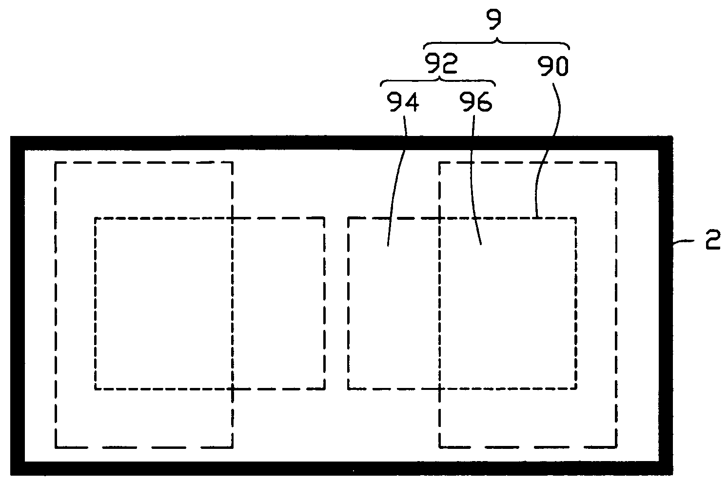
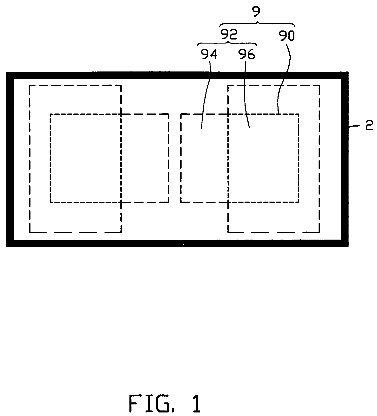
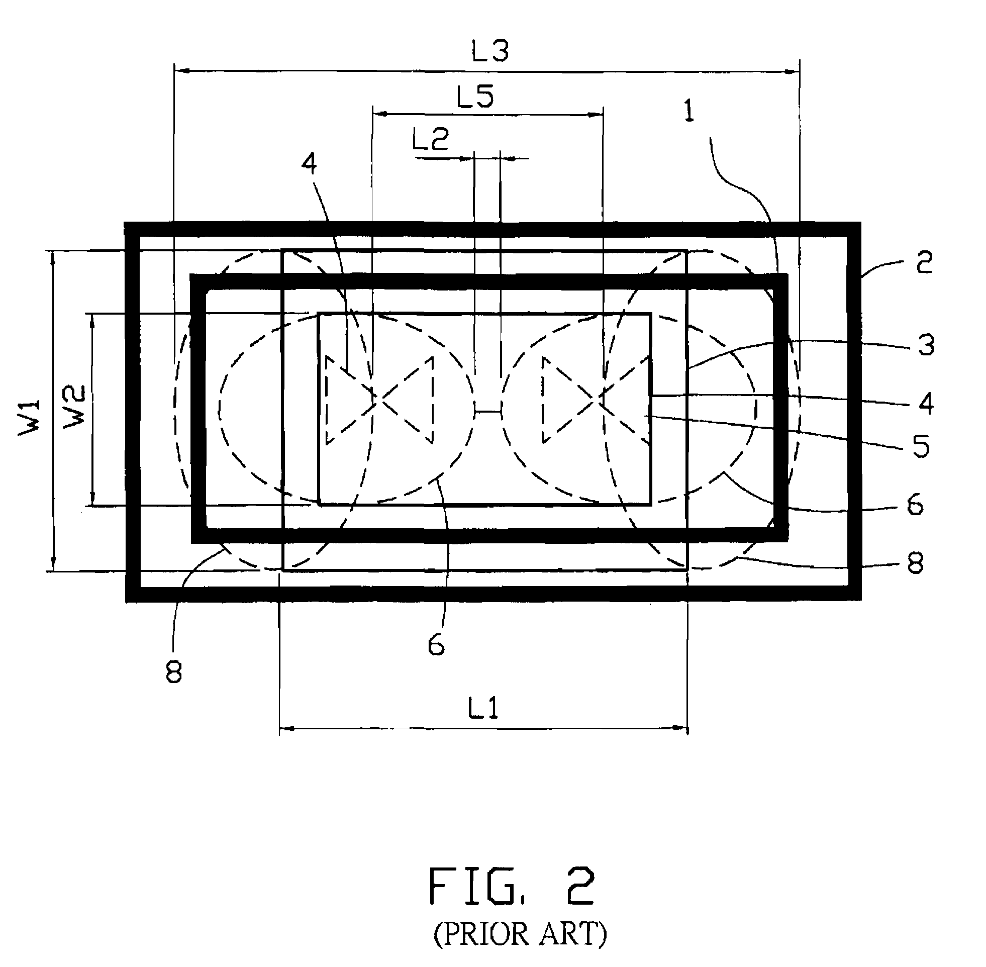
[0013]Referring to FIG. 1, a computer generated pad layout for a printed circuit board (PCB) according to a preferred embodiment of the present invention includes a pair of pads 9 for selectively receiving one of surface mounted components (SMCs) thereon. Referring also to FIG. 1, in the preferred embodiment, the pads 9 are for selectively receiving a 0805-type component 3 and a 0603-type component 5 thereon. The pair of pads 9 is arranged on the PCB. Each of the pads 9 is generally T-shaped, corresponding to a minimum sized shape that accommodates both a shape of the footprint of the 0805-type component 3 and a shape of the footprint of the 0603-type component 5.

[0014]By use of above described shapes, the surface area of the pads are minimized thereby reducing incidents of floating of small sized components, and reducing cost by minimizing materials used in manufacturing the pads. Further, in the design layout process of a PCB, by using pads shaped as described, a layout engineer w...


PUM


Abstract

A pad layout of a printed circuit board includes a first and a second pad symmetrically arranged on the PCB for cooperatively receiving either a first surface mounted component (SMC) or a second surface mounted component (SMC). Each of the SMCs includes a first footprint and a second footprint. The first pad has a polygonal shape corresponding to a minimum sized shape that accommodates both a shape of the first footprint of the first SMC and a shape of the first footprint of the second SMC. The second pad has a polygonal shape corresponding to a minimum sized shape that accommodates both a shape of the second footprint of the first SMC and a shape of the second footprint of the second SMC.

Description

BACKGROUND[0001]1. Technical Field[0002]Related subject matter is disclosed in a co-pending U.S. patent application Ser. No. 11 / 490,400, filed on Jul. 26, 2006, which is assigned to the same assignee as this application.[0003]The present invention relates to pad layouts of printed circuit boards (PCBs), and more particularly to a pad layout of a PCB which can readily and reliably receive surface mounted components (SMCs) thereon.[0004]2. General Background[0005]In general, SMCs, including resistors, capacitors, inductors and so on, are connected to a printed circuit board by pads. The pads are arranged on the printed circuit board in a matched relationship with footprints of the SMCs. The pads have different configurations due to varied configurations of the footprints of the SMCs, such as an ellipse, a circle, a square, a teardrop, and so on. Generally, however, the pad is only capable of receiving a certain SMC.[0006]Referring to FIG. 2, a pad layout of a printed circuit board (PC...

Claims


Application Information

Patent Timeline
Patent Type & Authority Patents(United States)
IPC IPC(8): G06F17/50H01R12/00H05K1/00
CPCH05K1/111H05K1/0295H05K2201/09381H05K2201/09954H05K2201/10636Y02P70/50
Inventor TAI, CHAN-FEIHUANG, YA-LING
Owner HONG FU JIN PRECISION IND (SHENZHEN) CO LTD
Why Eureka
Try Eureka