Flip chip light emitting diode devices having thinned or removed substrates

a light-emitting diode and flip-chip technology, applied in the field of electronic arts, can solve the problems of compromising device yield, difficult to achieve intimate bonding between the epitaxial layer stack and the transparent substrate over large areas, and reducing the thickness of the growth substrate of the device di

Active Publication Date: 2008-11-25
GE LIGHTING SOLUTIONS LLC
View PDF36 Cites 35 Cited by
  • Summary
  • Abstract
  • Description
  • Claims
  • Application Information

AI Technical Summary

Benefits of technology

[0009]According to one embodiment, a method is provided for fabricating a flip-chip light emitting diode device. Epitaxial layers are deposited on a growth substrate to produce an epitaxial wafer. A plurality of light emitting diode devices are fabricated on the epitaxial wafer. The epitaxial wafer is diced to generate a device die. The device die is flip chip bonded to a mount. The flip chip bonding includes securing the device die to the mount by bonding at least one electrode of the device die to at least one bonding pad of the mount. Subsequent to the flip chip bonding, a thickness of the growth substrate of the device die is reduced.
[0010]According to another embodiment, a method is provided for improving light emission of a flip-chip bonded light emitting diode device that is flip chip bonded to a mount. A growth substrate of the light emitting diode device is thinned or removed. The growth substrate of the flip-chip bonded light emitting diode device is arranged distal from the mount. The thinning or removing is performed while epitaxial layers of the light emitting diode device are flip chip bonded to the mount. The flip chip bonding effects a securing of the light emitting diode device to the mount during the thinning or removing.
[0011]According to yet another embodiment, a flip-chip light emitting diode device is disclosed. A mount includes bonding bumps. A light emitting diode device die has a device layers stack that is flip chip bonded to the bonding bumps of the mount. An underfill material is arranged between the light emitting diode device die and the mount. The underfill material supports the light emitting diode device die and prevents the light emitting diode device die from fracturing.

Problems solved by technology

A problem can arise in the flip-chip configuration when the growth substrate is substantially light-absorbing over some or all of the spectral range of light emission.
Moreover, even if a suitable optically transparent substrate is available, such as is the case for group III-nitride light emitting diodes which can be grown on a transparent sapphire growth substrate, reflection optical losses can occur at the interface between the substrate and the epitaxial layers due to an abrupt discontinuity in refractive index.
However, achieving intimate bonding between the epitaxial layers stack and the transparent substrate over large areas is difficult.
Device yield can be compromised due to the formation of air bubbles or the presence of particles at the interface between the epitaxial layers stack and the transparent substrate during the bonding.
Moreover, absent a close refractive index match between the epitaxial layers stack and the transparent substrate, reflections at the interface between the layers stack and the transparent wafer can introduce optical losses.
However, the epitaxial layers stack and the remaining thinned growth substrate form a fragile structure after growth substrate thinning.
The fragility of this thinned structure complicates the further processing, dicing, and flip chip bonding, resulting in lowered device yield.
Moreover, air bubbles, particles, or other imperfections in the adhesion between the temporary support wafer and the epitaxial layers stack can introduce localized damage to the thinned structure, also impacting device yield.

Method used


Image

  • Flip chip light emitting diode devices having thinned or removed substrates
  • Flip chip light emitting diode devices having thinned or removed substrates
  • Flip chip light emitting diode devices having thinned or removed substrates

Examples


Embodiment Construction

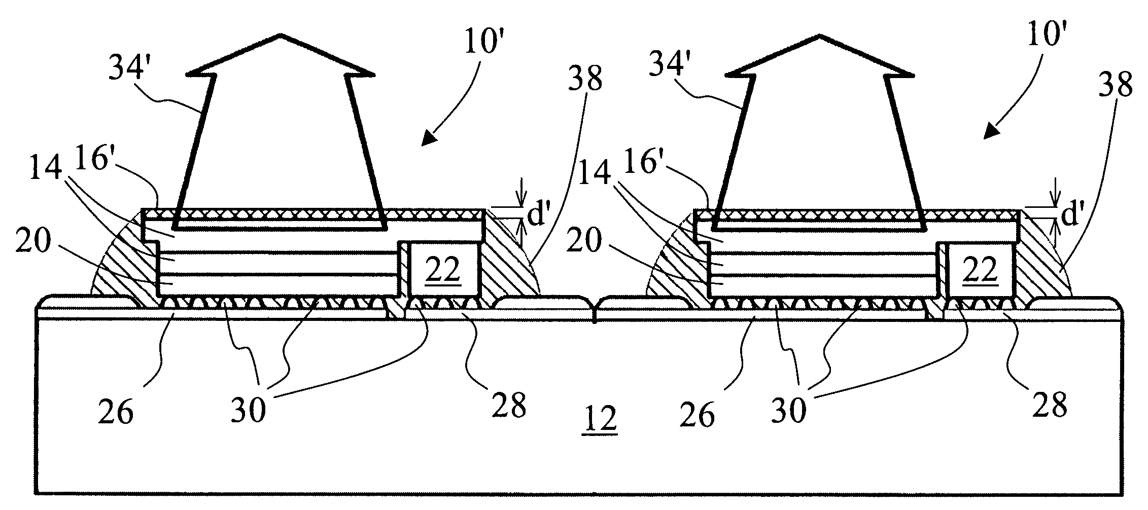
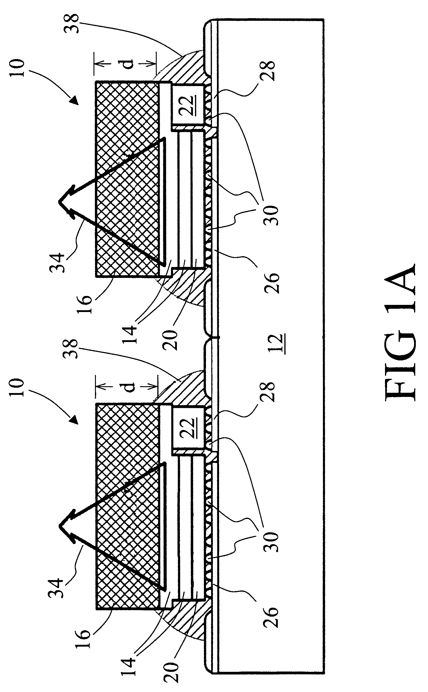
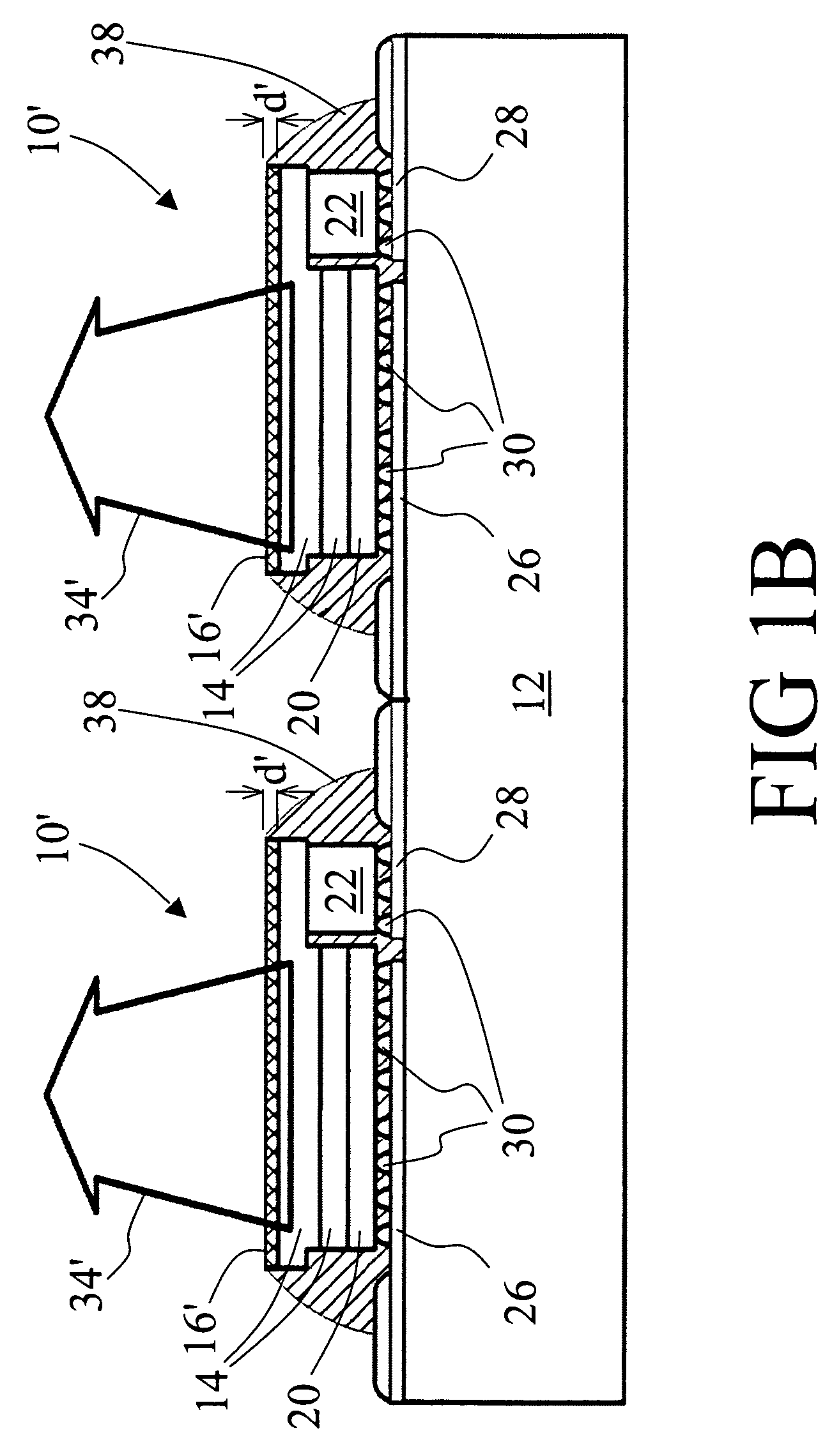
[0020]With reference to FIG. 1A, two exemplary flip chip bonded light emitting diode device die 10 are shown mounted in flip-chip fashion on a mount 12. Each exemplary light emitting diode device die 10 includes a semiconductor device layers stack 14 that is epitaxially deposited on a growth substrate 16. The epitaxial device layers stack 14 defines a light emitting diode device such as a group III nitride ultraviolet or blue light emitting diode, a group III phosphide visible-emission light emitting diode, a group III arsenide vertical cavity surface emitting laser diode, or the like.

[0021]In FIG. 1A, the semiconductor layers stack 14 has two exemplary layers corresponding to a simple p / n diode; however, those skilled in the art will appreciate that more complex semiconductor layers stacks can be employed. In a vertical cavity surface emitting laser diode, for example, the layers stack can include dozens of layers that define Bragg reflectors, claddings, and a complex multi-quantum...


PUM


Abstract

In a method for fabricating a flip-chip light emitting diode device, epitaxial layers (14, 114) are deposited on a growth substrate (16, 116) to produce an epitaxial wafer. A plurality of light emitting diode devices are fabricated on the epitaxial wafer. The epitaxial wafer is diced to generate a device die (10, 110). The device die (10, 110) is flip chip bonded to a mount (12, 112). The flip chip bonding includes securing the device die (10, 110) to the mount (12, 112) by bonding at least one electrode (20, 22, 120) of the device die (10, 110) to at least one bonding pad (26, 28, 126) of the mount (12, 112). Subsequent to the flip chip bonding, a thickness of the growth substrate (16, 116) of the device die (10, 110) is reduced.

Description

[0001]This application claims the benefit of U.S. Provisional Application Ser. No. 60 / 490,761 filed on Jul. 29, 2003.BACKGROUND[0002]The present invention relates to the electronics arts. It is especially relates to group III-nitride flip-chip bonded light emitting diodes for lighting applications, and will be described with particular reference thereto. However, the invention also finds application in conjunction with other types of flip-chip bonded light emitting diodes, and in other flip-chip bonded epitaxial semiconductor devices such as vertical cavity surface emitting laser diodes.[0003]In the flip-chip mounting configuration, a light emitting diode with a light-transmissive substrate and front-side electrodes is bonded “face down” to bonding bumps of a mount, that is, with the epitaxial layers proximate to the mount and the light-transmissive substrate distal from the mount. The flip-chip arrangement has a number of advantages, including improved thermal heat sinking due to t...

Claims


Application Information

Patent Timeline
Patent Type & Authority Patents(United States)
IPC IPC(8): H01L21/00H01L25/075H01L33/00H01L33/62
CPCH01L25/0753H01L33/0079H01L33/62H01L2224/16H01L2224/48091H01L2924/00014H01L33/0093
Inventor ELIASHEVICH, IVANKOLODIN, BORISSTEFANOV, EMIL P.
Owner GE LIGHTING SOLUTIONS LLC
Why Eureka
Try Eureka