Write apparatus for DDR SDRAM semiconductor memory device

a technology of semiconductor memory and write apparatus, which is applied in the direction of information storage, static storage, digital storage, etc., can solve the problems of increasing power consumption, and achieve the effect of reducing the number of data lines and the number of latches

Active Publication Date: 2008-12-09
SK HYNIX INC
View PDF11 Cites 43 Cited by
  • Summary
  • Abstract
  • Description
  • Claims
  • Application Information

AI Technical Summary

Benefits of technology

[0005]Accordingly, the present invention provides a writing apparatus capable of reducing the number of data lines and the number of latches at the time of a writing operation.

Problems solved by technology

Furthermore, since the number of operating circuits increases, power consumption is increased.

Method used


Image

  • Write apparatus for DDR SDRAM semiconductor memory device
  • Write apparatus for DDR SDRAM semiconductor memory device
  • Write apparatus for DDR SDRAM semiconductor memory device

Examples


Embodiment Construction

[0019]Now, specific embodiments according to the present patent will be described with reference to the accompanying drawings.

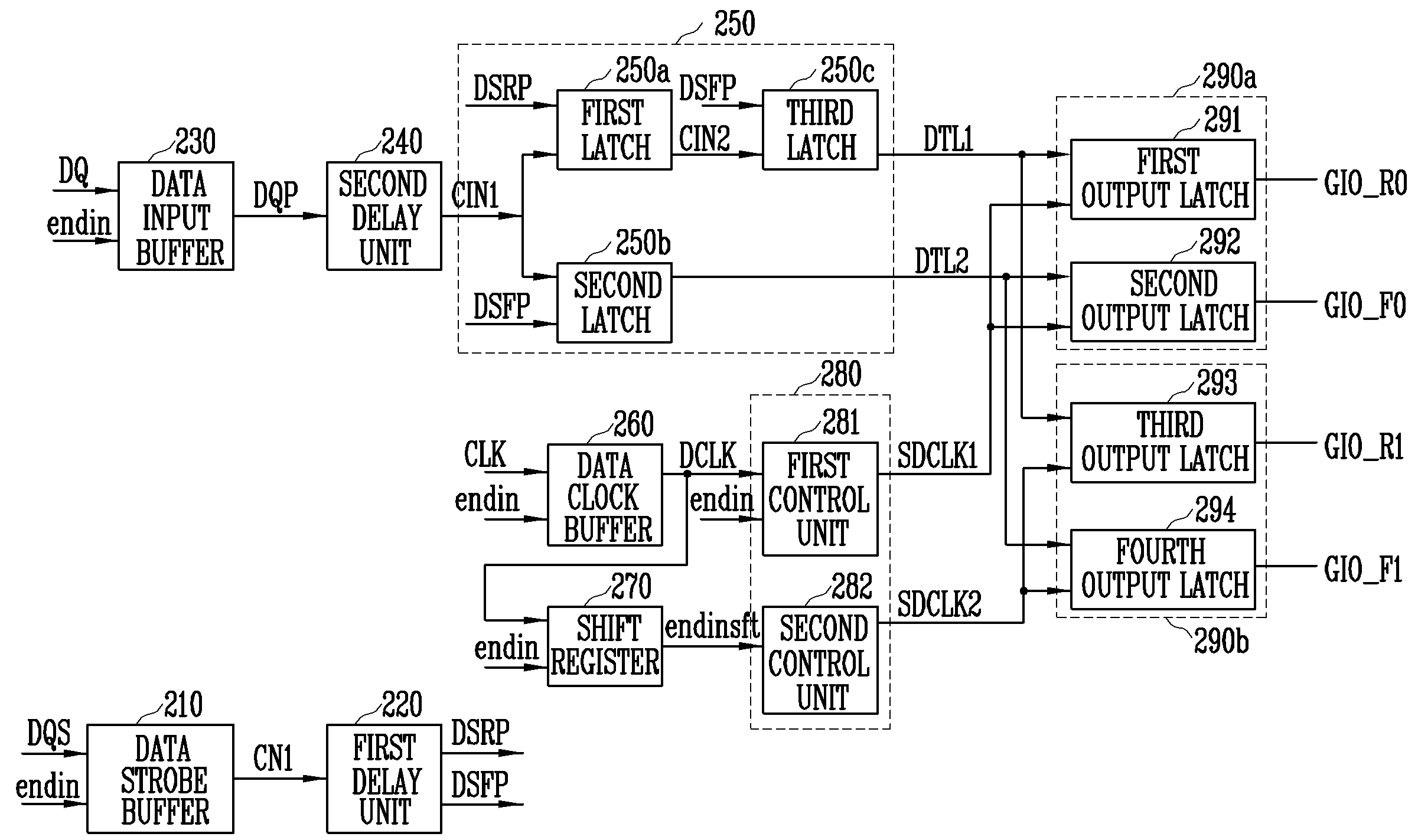
[0020]FIG. 3 is a schematic block diagram of a data write apparatus in DDR SDRAM according to the present invention. The write apparatus includes a data strobe buffer 210, a first delay unit 220, a data input buffer 230, a second delay unit 240, a latch unit 250, a data clock buffer 260, a shift register 270, a control unit 280, a first output latch unit 290a and a second output latch unit 290b. The data strobe buffer 210 buffers a data strobe pulse DQS and outputs a first transfer signal CN1 in response to an enable signal endin. The first delay unit 220 outputs a rising sense signal DSRP and a falling sense signal DSFP in response to the first transfer signal CN1. The data input buffer 230 receives data through an input terminal DQ, buffers the data and outputs a second transfer signal CN2 in response to an enable signal endin. The second delay unit 240 tra...


PUM


Abstract

A writing apparatus of a semiconductor memory device includes a pulse generator, a latch unit and an output latch unit. The pulse generator outputs a first pulse every rising edge of a data strobe pulse and a second pulse every falling edge of the data strobe pulse, respectively. The latch unit latches data input every rising edge of the first pulse, latches data input every rising edge of the second pulse and the latched data, respectively, and allocates the latched data to first and second data lines. The output latch unit latches data, which are firstly allocated to the first and second data lines, in response to a first control signal, and latches data, which are secondly allocated to the first and second data lines, in response to a second control signal.

Description

CROSS-REFERENCES TO RELATED APPLICATIONS[0001]The present application claims priority to Korean patent application number 10-2006-034984, filed on Apr. 18, 2006, which is incorporated by reference in its entirety.BACKGROUND OF THE INVENTION[0002]The present invention relates, in general, to semiconductor memory devices and, more particularly, to a write apparatus of Double Data Rate Synchronous DRAM (DDR SDRAM).[0003]Recently, DDR SDRAM has been in the spotlight since it has a high operating speed compared with conventional SDRAM. In general, in DDR SDRAM, data are input and output in synchronization with the rising or falling edge of a clock. However, four register signals must be latched in parallel. It increases the number of signals, resulting in an increased area of the circuit. Furthermore, since the number of operating circuits is increased, a necessary amount of current is increased.[0004]FIG. 1 is a block diagram schematically showing a data write apparatus in conventional ...

Claims


Application Information

Patent Timeline
Patent Type & Authority Patents(United States)
IPC IPC(8): G11C7/10
CPCG11C7/1039G11C7/1066G11C7/1072G11C7/1078G11C7/1087G11C7/1093G11C7/1096
Inventor KU, KIE BONGCHO, KWANG JUN
Owner SK HYNIX INC
Why Eureka
Try Eureka