Method for designing alternating phase shift masks

a phase shift mask and phase width technology, applied in the field of mask manufacturing, can solve the problems of time-consuming decreased light intensity, unwanted patterns on the wafer, etc., and achieve the effect of reducing shape complexity, eliminating phase width or spacing violations, and eliminating lengthy and error-prone iterative cleanup

Inactive Publication Date: 2008-12-30
GLOBALFOUNDRIES INC
View PDF7 Cites 4 Cited by
  • Summary
  • Abstract
  • Description
  • Claims
  • Application Information

AI Technical Summary

Benefits of technology

[0012]It is another object of the present invention to provide a method of designing altPSMs that eliminates phase width or spacing violations.
[0013]A further object of the invention is to provide a method of designing altPSMs that eliminates lengthy and error prone iterative cleanup in small steps, while minimizing shape complexity and avoiding topological phase errors caused by overly aggressive phase shape cleanup.

Problems solved by technology

However, since the recessed regions on the mask have to form closed polygons and not all edges of these polygons can be made to coincide with desired layout images, the light intensity decrease caused by these residual 180° phase steps leads to unwanted patterns on the wafer.
One of the major challenges in generating an altPSM layout is to create manufacturable and lithographically viable phase shapes without introducing undue layout conflicts.
Since every expansion can lead to new spacing violations and every fill operation can lead to new width violations, phase shape legalization has to be done iteratively.
However, since these portions still violate the minimum width rule vertically, and now also add a further minimum width violation horizontally, additional expansion is made by adding portions both below and to the side in several steps.
This iterative cleanup is time consuming and error prone.
It is impossible to predict the exact number of iterations required, and most CAD tools do not support looping.
This was attempted previously in router based altPSM deisgns However, router-based altPSM designs have the disadvantage that they do not carry a preferred orientation of the phase transitions through the entire layout segment, and instead force closed loops.
This detracts from good lithographic performance.

Method used


Image

  • Method for designing alternating phase shift masks
  • Method for designing alternating phase shift masks
  • Method for designing alternating phase shift masks

Examples


Embodiment Construction

)

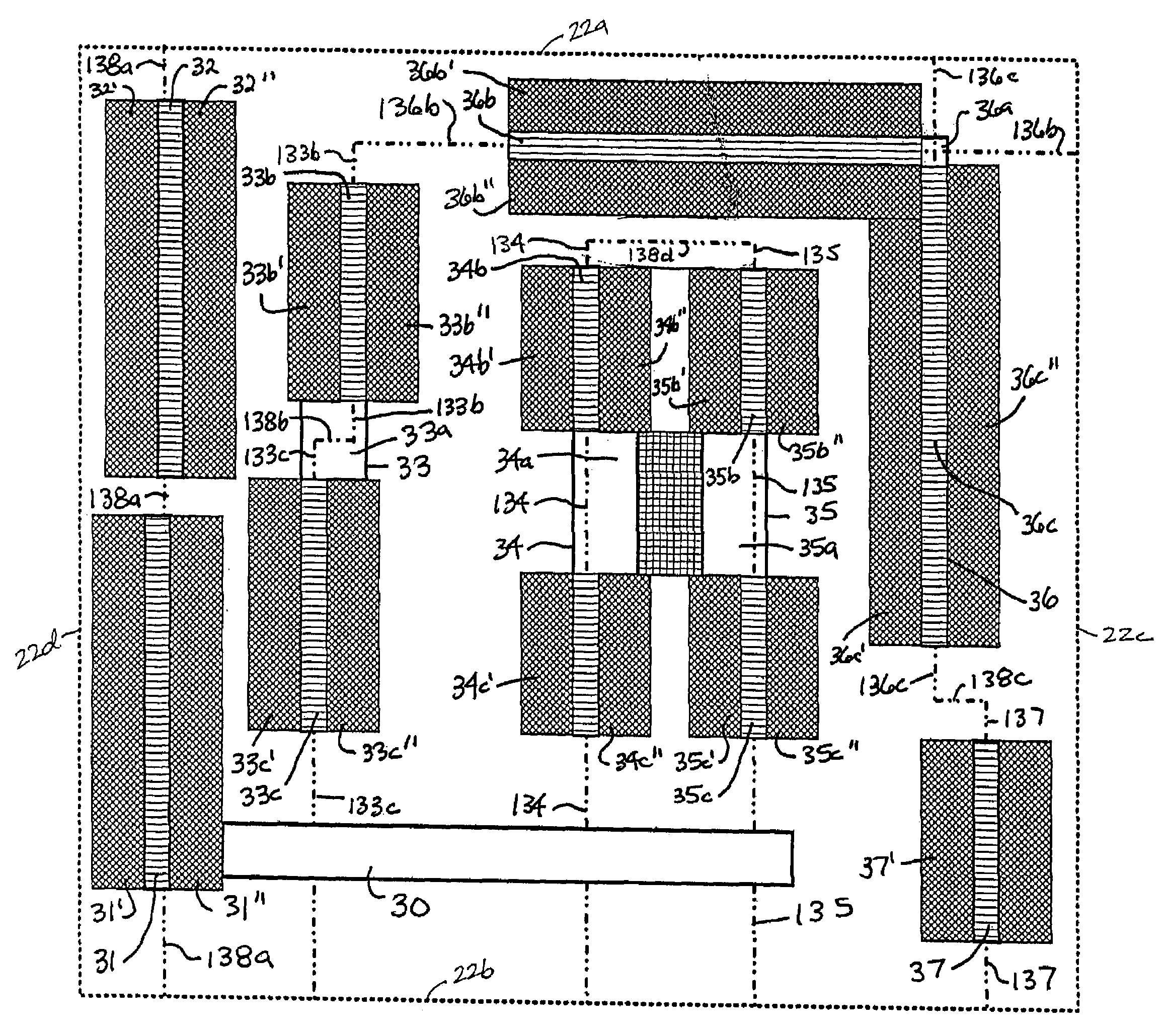
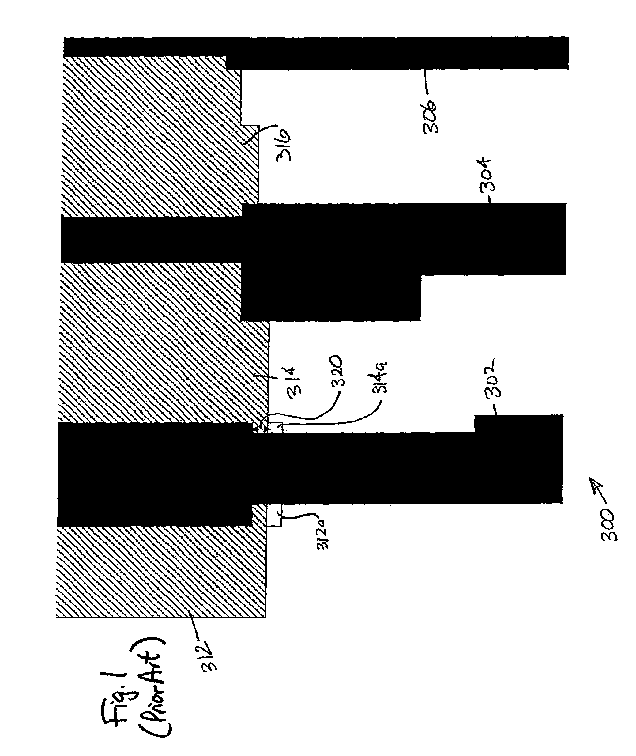
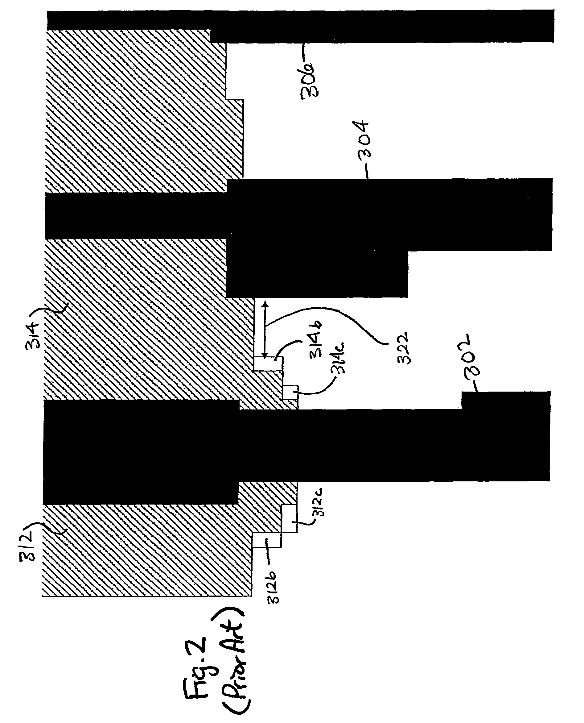
[0045]In describing the preferred embodiment of the present invention, reference will be made herein to FIGS. 4-19 of the drawings in which like numerals refer to like features of the invention.

[0046]A method and computer system is described for designing an alternating phase shifting mask for projecting an image of an integrated circuit design. In the preferred method the design commences by organizing the initial circuit design pattern layout into discrete regions containing phase dependencies, and within each phase dependent region, dividing the region into relatively simply shaped polygons for phase shift regions that obey the lithographic and manufacturability constraints while avoiding layout conflicts. The resulting altPSM layouts have improved accuracy, efficiency, and lithographic performance compared to altPSM layouts using conventional design methodologies. FIG. 18 illustrates a flowchart of a preferred embodiment of the method 200 for designing an altPSM layout design i...


PUM

PropertyMeasurementUnit
critical dimensionaaaaaaaaaa
distanceaaaaaaaaaa
lengthaaaaaaaaaa

Abstract

A method of designing an alternating phase shifting mask for projecting an image of an integrated circuit design having a plurality of spaced segments of critical dimension. The method initially identifies a phase universe boundary, such that the phase universe comprises a contiguous region of the integrated circuit layout wherein critical dimension segments within the phase universe are beyond a maximum phase interaction distance from any critical dimension segments outside the phase universe in accordance with predetermined design rules. The method then divides the phase universe into phase regions separated by the integrated circuit layout and any extensions of the critical dimension segments so that the phase regions are binary colorable within the phase universe.

Description

BACKGROUND OF THE INVENTION[0001]1. Field of the Invention[0002]The present invention is directed to the manufacture of masks used in the lithographic production of integrated circuits and, in particular, to the manufacture of phase shifting masks (PSMs).[0003]2. Description of Related Art[0004]As an alternative to chrome on glass (COG) masks used in the lithographic production of integrated circuits, alternating phase shifting masks (altPSMs) have been employed in order to increase the resolution of the critical active area patterns projected. Such increased resolution enables smaller line widths to be exposed on the resist and consequently etched into or deposited on the wafer substrate. The critical dimension (CD) of the system is the smallest dimension that the lithographic system can create on the resist layer by normal techniques, and altPSMs permit sub-CD widths to be exposed and created on the wafer. This is done by manipulating the electric field vector or phase of the ener...

Claims


Application Information

Patent Timeline
Patent Type & Authority Patents(United States)
IPC IPC(8): G03F1/00G06F17/50
CPCG03F1/30
Inventor LIEBMANN, LARS WFONSECA, CARLOS A
Owner GLOBALFOUNDRIES INC
Why Eureka
Try Eureka