Magnetic random access memory (MRAM) having a magnetic tunneling junction (MTJ) layer including a tunneling film of uniform thickness and method of manufacturing the same

a random access memory and magnetic tunneling junction technology, applied in the field of magnetic tunneling junctions (mtj) layers including a uniform thickness tunneling film, can solve the problems of reducing the reliability of the conventional mram device, affecting the reliability of the mram, and preserving data for a relatively long time. the effect of cell resistance and mr reduction, increased insulation breakdown voltage and reduced resistance deviation between cells

Active Publication Date: 2009-01-06
SAMSUNG ELECTRONICS CO LTD
View PDF17 Cites 16 Cited by
  • Summary
  • Abstract
  • Description
  • Claims
  • Application Information

AI Technical Summary

Benefits of technology

[0021]It is a feature of an embodiment of the present invention to provide a magnetic random access memory having a magnetic tunneling junction (MTJ) layer including a tunneling film of uniform thickness, and a method of manufacturing the same, that is able to reduce resistance deviation between cells, increase cell resistance and MR, and increase an insulation breakdown voltage.
[0022]It is another feature of an embodiment of the present invention to provide a magnetic random access memory having a magnetic tunneling junction (MTJ) layer including a tunneling film of uniform thickness, and a method of manufacturing the same, that is able to reduce the shift of the magnetic field of a free ferromagnetic film and the coercivity of the free ferromagnetic film, thereby recording and reading data more reliably.
[0034]In an MRAM according to an embodiment of the present invention, since the tunneling film has a uniform thickness and a substantially flat upper surface, i.e., without waves, resistance deviation between cells may be reduced, cell resistance and MR may be increased, and insulation breakdown voltage may be increased. Further, since a shift magnetic field HN due to Neel coupling can be reduced, the shift of the magnetic field of a free ferromagnetic film and the coercivity of the free ferromagnetic film may be reduced. Therefore, data is recorded and read more reliably.

Problems solved by technology

In addition, MRAM can maintain data for a relatively long time without a refreshing process, similar to a flash memory device.
If the thickness of the tunneling film S4 is not uniform, a thin area may cause a weak point.
A second drawback of the conventional MRAM is that the tunneling film S4 is not flat. FIG. 4 is a schematic showing Neel coupling caused by waves, i.e., an uneven upper surface, in the tunneling oxide film S4 of the conventional MTJ layer depicted in FIG. 2.
This problem may cause an error in the recording or reading of data.
This results in errors in recording or reading data of the MTJ layer, thereby diminishing the reliability of the conventional MRAM device.

Method used


Image

  • Magnetic random access memory (MRAM) having a magnetic tunneling junction (MTJ) layer including a tunneling film of uniform thickness and method of manufacturing the same
  • Magnetic random access memory (MRAM) having a magnetic tunneling junction (MTJ) layer including a tunneling film of uniform thickness and method of manufacturing the same
  • Magnetic random access memory (MRAM) having a magnetic tunneling junction (MTJ) layer including a tunneling film of uniform thickness and method of manufacturing the same

Examples


first embodiment

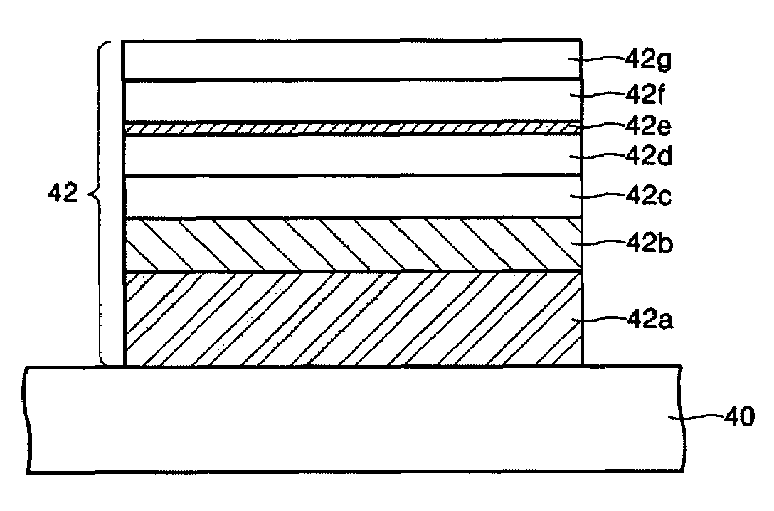
[0075]FIGS. 13 and 14 illustrate cross-sectional views of stages in a method of forming an MRAM according to the present invention. Referring to FIG. 13, the lower electrode 42a is formed on the conductive pad layer 40 connected to a source region of a MOSFET. The lower electrode 42a may be formed of a conductive, e.g., metal, electrode made of a single film or a stacked double film. When the lower electrode 42a is formed of a single film, it is preferably formed of a metal such as tantalum, but may be formed of another metal. When the lower electrode 42a is formed of a double film, it is preferably formed of metals such as tantalum / ruthenium, but may be formed of other metals. The flattening film 42b is formed on the lower electrode 42a to a predetermined thickness. The flattening film 42b can be used as a part of the lower electrode. In this case, the lower electrode 42a is a first lower electrode, and the flattening film 42b is a second lower electrode. The flattening film 42b ma...

second embodiment

[0079]FIGS. 15 through 17 illustrate cross-sectional views of stages in a method of forming an MRAM according to the present invention. Referring to FIG. 15, a lower electrode 60 is formed on the conductive pad layer 40. The lower electrode 60 may be formed of a metal compound electrode, such as a titanium nitride (TiN) electrode. Subsequently, an upper surface of the lower electrode 60 is flattened. While it is preferable to use a chemical mechanical polishing method to flatten the upper surface of the lower electrode 60, other flattening methods may be used.

[0080]Referring now to FIG. 16, after flattening the upper surface of the lower electrode 60, the flattening film 42b is formed on the lower electrode 60. Then, the pinning and pinned ferromagnetic films 42c and 42d, the tunneling film 42e, the free ferromagnetic film 42f, and the capping film 42g, are formed sequentially. Next, a second photosensitive film PR2 is formed on the capping film 42g. Then, the stacked films are sequ...


PUM

PropertyMeasurementUnit
insulation breakdown voltageaaaaaaaaaa
thicknessaaaaaaaaaa

Abstract

A magnetic random access memory (MRAM), and a method of manufacturing the same, includes a cell including a transistor and a magnetic tunneling junction (MTJ) layer connected to the transistor, wherein the MTJ layer includes a lower electrode, a lower magnetic film, a tunneling film having a uniform thickness and a substantially flat upper surface, and an upper magnetic film, wherein the lower electrode includes a first lower electrode and an amorphous second lower electrode. An amorphous flattening film may be further formed between the lower electrode and the lower magnetic film.

Description

BACKGROUND OF THE INVENTION[0001]1. Field of the Invention[0002]The present invention relates to a semiconductor memory device and a method of manufacturing the same. More particularly, the present invention relates to a magnetic random access memory having a magnetic tunneling junction (MTJ) layer including a tunneling film of uniform thickness and a method of manufacturing the same.[0003]2. Description of the Related Art[0004]A magnetic random access memory (MRAM) is a memory device used to read and write data utilizing a property of resistance variation of a magnetic tunneling junction (MTJ) cell depending on a direction of magnetization of the MTJ cell. The MTJ cell includes a tunneling film and magnetic films on and under an insulating film.[0005]MRAM is as highly integrated as a dynamic random access memory (DRAM) and capable of operating at high speed like a static random access memory (SRAM). In addition, MRAM can maintain data for a relatively long time without a refreshing...

Claims


Application Information

Patent Timeline
Patent Type & Authority Patents(United States)
IPC IPC(8): G11C11/15G11C11/16H01F10/06H01F10/32H01F41/30H01L21/8246H01L27/105H01L27/115H01L43/08H01L43/12
CPCB82Y10/00B82Y25/00B82Y40/00G11C11/16H01F10/06H01F10/3254H01F41/308H01L27/228H01L43/08H01L43/12H10B61/22H10N50/10H10N50/01H10B69/00
Inventor KIM, TAE-WANPARK, SANG-JIN
Owner SAMSUNG ELECTRONICS CO LTD
Why Eureka
Try Eureka