
System and method to facilitate time domain sampling for solid state imager

Active Publication Date: 2009-01-06
TEXAS INSTR INC
View PDF9 Cites 8 Cited by
  • Summary
  • Abstract
  • Description
  • Claims
  • Application Information

AI Technical Summary

Benefits of technology

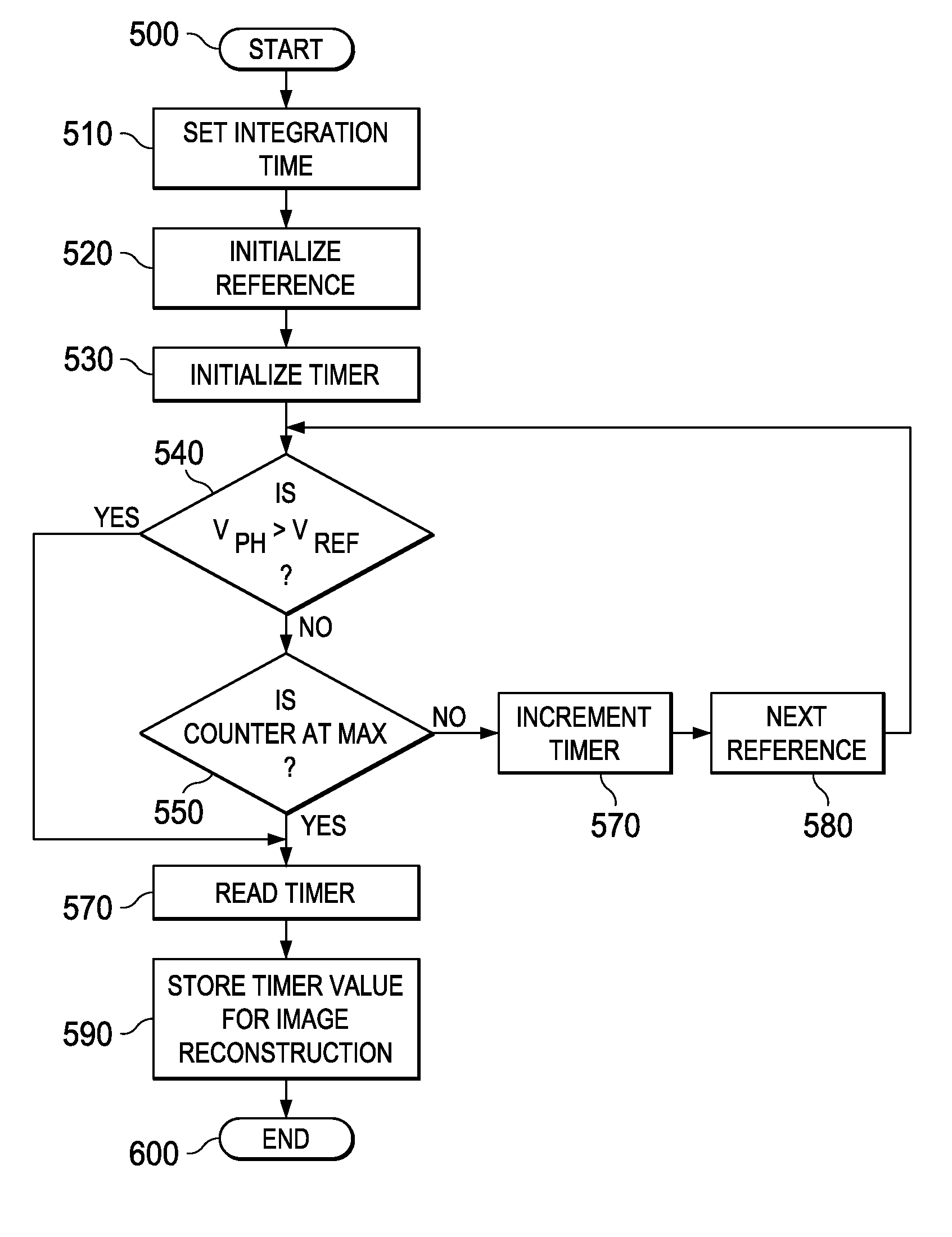
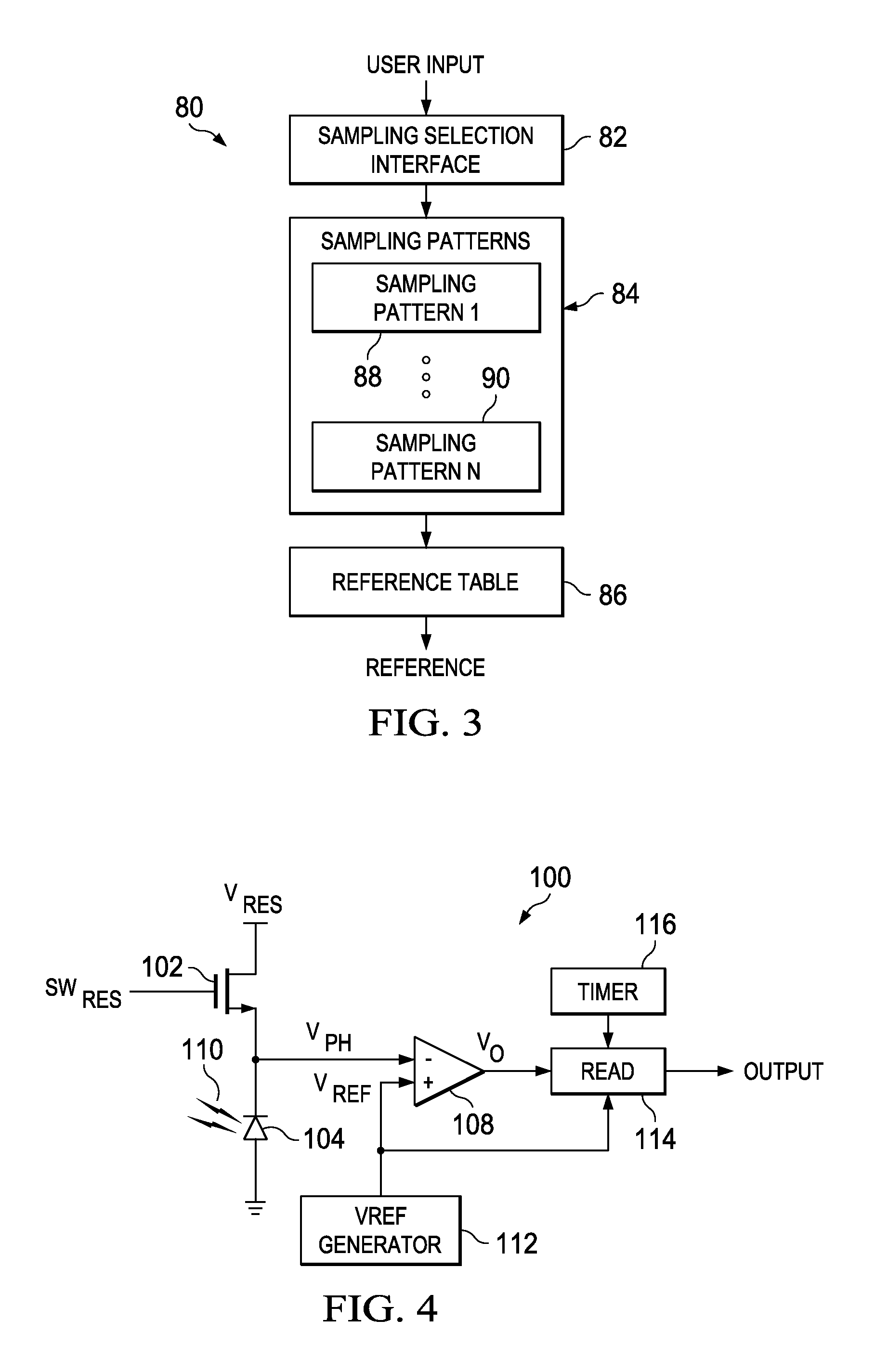
[0012]In accordance with a particular aspect of the present invention, application-dependent, three-dimensional parameters, such as photocurrent, integration time, and reference voltage, can be derived according to a search method to facilitate image capture so as to provide a wide dynamic range and reasonable resolution imaging. One or more of such parameters can be programmable for a given application. The proposed imaging technique thus provides controllable and flexible sampling patterns.

Problems solved by technology

However, CCD-based image sensors are limited or impractical for use in many consumer applications.
CCDs thus cannot be fabricated employing conventional Complimentary-Symmetry Metal-Oxide Semiconductor (CMOS) fabrication processes.
The mismatch in processing technology for CCDs also precludes the integration of additional on-chip functionality beyond light sensing and charge to voltage conversion for CCDs.
The operation of CCD imagers also requires multiple high supply voltages (e.g., 5V-12V) resulting in higher power consumption than CMOS imagers.
As a result, the costs for the CCD image sensor and the system employing the sensor remain high.
Additionally, since the current to charge the CCDs is high, CCDs are not well suited for portable devices.
The logarithmic response technique suffers from the problem of fixed pattern noise due to the device mismatches, and poor sensitivity and local contrast.
This technique suffers from mismatch in the lateral overflow transistor gate-drain overlap capacitance.
Also it requires capturing multiple frames and complex reconstruction processing.
Furthermore, its logarithmic compression curve strongly reduces image contrast.
Floating-point pixel-level ADC imagers require large memory to store the data and require a complex reconstruction process.
However, the readout process of the photosensor array generally takes a very long time.
Thus, this technique is not applicable for many implementations.
This technique requires a constant reference voltage and the imaging procedure requires a full second of time.
Also, since a pixel is read off-chip multiple times, the power consumption of the system can be substantial.

Method used


Image

  • System and method to facilitate time domain sampling for solid state imager
  • System and method to facilitate time domain sampling for solid state imager
  • System and method to facilitate time domain sampling for solid state imager

Examples


Embodiment Construction

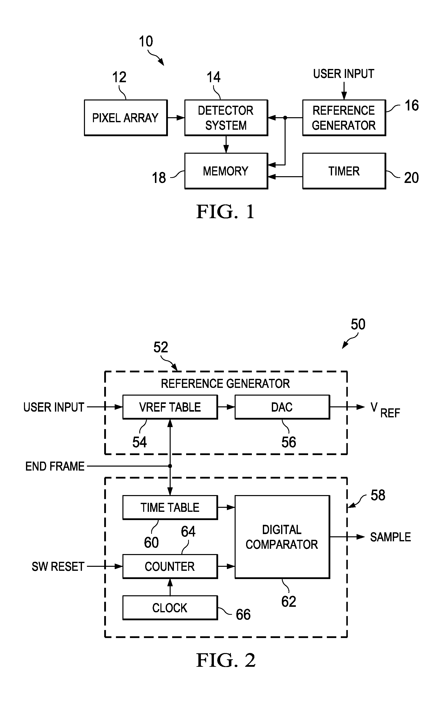
[0031]The present invention relates generally to a time domain sampling technique for a CMOS imager. The present approach enables a wide dynamic range and flexibility due to employing two-degrees of freedom during such sampling. Two degrees of freedom can be achieved by making one or both of an integration time and a reference (e.g., voltage or current) variable during sampling. The time domain sampling with the CMOS image sensor is implemented by storing a time associated with when a pixel has a desired value relative to a reference in response to the pixel receiving incident light. The reference can be fixed or variable over time, and further can be programmable to implement a desired sampling pattern for a given application.

[0032]FIG. 1 illustrates an imaging system 10 to facilitate sampling in the time domain in accordance with the aspect of the present invention. The system 10 includes a pixel array 12 having a plurality of pixels, such as arranged in the plurality of rows and ...


PUM


Abstract

A time domain sampling technique for a CMOS imager enables a wide dynamic range and flexibility by employing up to two-degrees of freedom during such sampling. Two degrees of freedom can be achieved by making one or both of an integration time and a reference (e.g., voltage or current) variable during sampling. The sampling (or image capture) is implemented by associating a time with when a pixel has a desired value relative to the reference in response to the pixel receiving incident light. The reference can be fixed or variable during different portions of the sampling, and further can be programmable to implement a desired sampling pattern for a given application.

Description

CROSS REFERENCE TO RELATED APPLICATION[0001]The present application claims the benefit of U.S. Provisional Patent Application Serial No. 60 / 335,202, filed Oct. 24, 2001, entitled TWO-DEGREE OF FREEDOM TIME DOMAIN SAMPLING TECHNIQUE FOR CMOS IMAGER, and which is incorporated herein by reference.TECHNICAL FIELD[0002]The present invention relates to imaging and more particularly to a system and method to facilitate time domain sampling for a solid state imager.BACKGROUND OF INVENTION[0003]Imaging systems are employed in a variety of applications, such as medical devices, satellite as well as microscope and telescope apparatuses. More recently, imaging systems have been utilized in a variety of additional applications such as digital cameras, computer scanners and digital camcorders. A majority of these applications utilize charge-coupled-devices (CCDs) as the underlying image sensors. However, CCD-based image sensors are limited or impractical for use in many consumer applications.[000...

Claims


Application Information

Patent Timeline
IPC IPC(8): H04N3/14H04N5/335H04N5/353H04N5/355H04N5/374H04N5/378
CPCH04N3/155H04N5/335H04N25/00
Inventor LUO, QIANGCHEN, ZHILIANG JULIANHARRIS, JOHN G.CLYNES, STEVEERWIN, MICHAEL
Owner TEXAS INSTR INC
Learn More