Ion beam angle measurement systems and methods employing varied angle slot arrays for ion implantation systems

a technology of ion beam and measurement system, which is applied in the field of ion beam angle measurement system, can solve the problems of unintended depth, unfavorable modification of implantation profile, damage to device structure, etc., and achieve the effect of facilitating semiconductor device fabrication

Active Publication Date: 2009-01-13
AXCELIS TECHNOLOGIES
View PDF23 Cites 2 Cited by
  • Summary
  • Abstract
  • Description
  • Claims
  • Application Information

AI Technical Summary

Benefits of technology

[0009]The present invention facilitates semiconductor device fabrication by detecting or measuring angle of incidence values for incident ion beams and optionally correcting angular errors before and / or during ion implantation procedures. The present invention employs varied angle slot arrays comprised of structures having a plurality of slots defined therein. The slot arrays select one or more beamlets from ion beams according to varied acceptance angles. Charge measurement sensors, such as pickup sensors, measure charge or beam current associated with each of the slots of the array. From these measurements and acceptance angles for each of the slots, an angle of incidence value for the ion beam can be obtained.

Problems solved by technology

Such errors can undesirably modify the implantation profile, fail to dope certain areas, implant dopants into unintended areas, damage device structures, dope to an incorrect depth, and the like.

Method used


Image

  • Ion beam angle measurement systems and methods employing varied angle slot arrays for ion implantation systems
  • Ion beam angle measurement systems and methods employing varied angle slot arrays for ion implantation systems
  • Ion beam angle measurement systems and methods employing varied angle slot arrays for ion implantation systems

Examples


Embodiment Construction

[0022]The present invention will now be described with reference to the attached drawings, wherein like reference numerals are used to refer to like elements throughout. It will be appreciated by those skilled in the art that the invention is not limited to the exemplary implementations and aspects illustrated and described hereinafter.

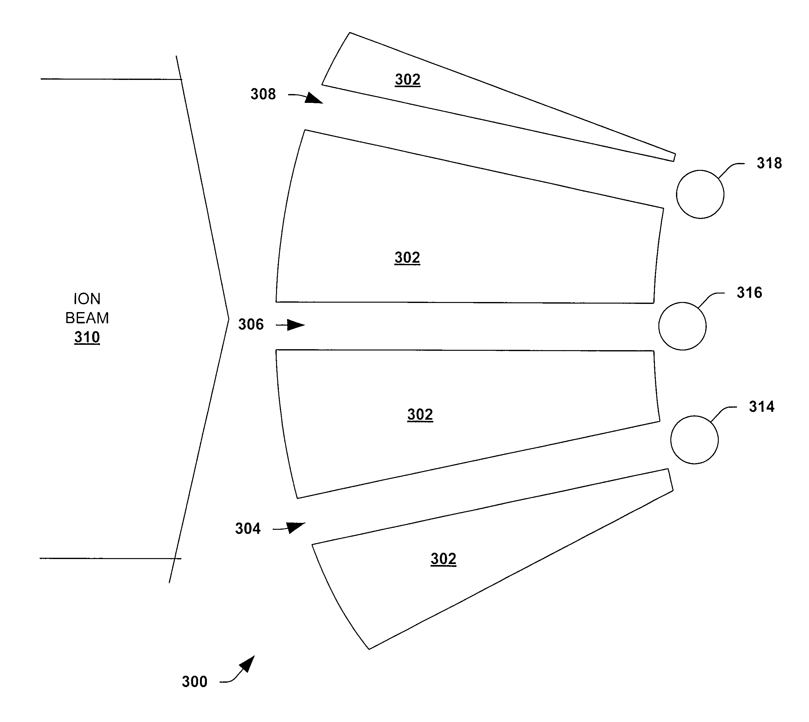
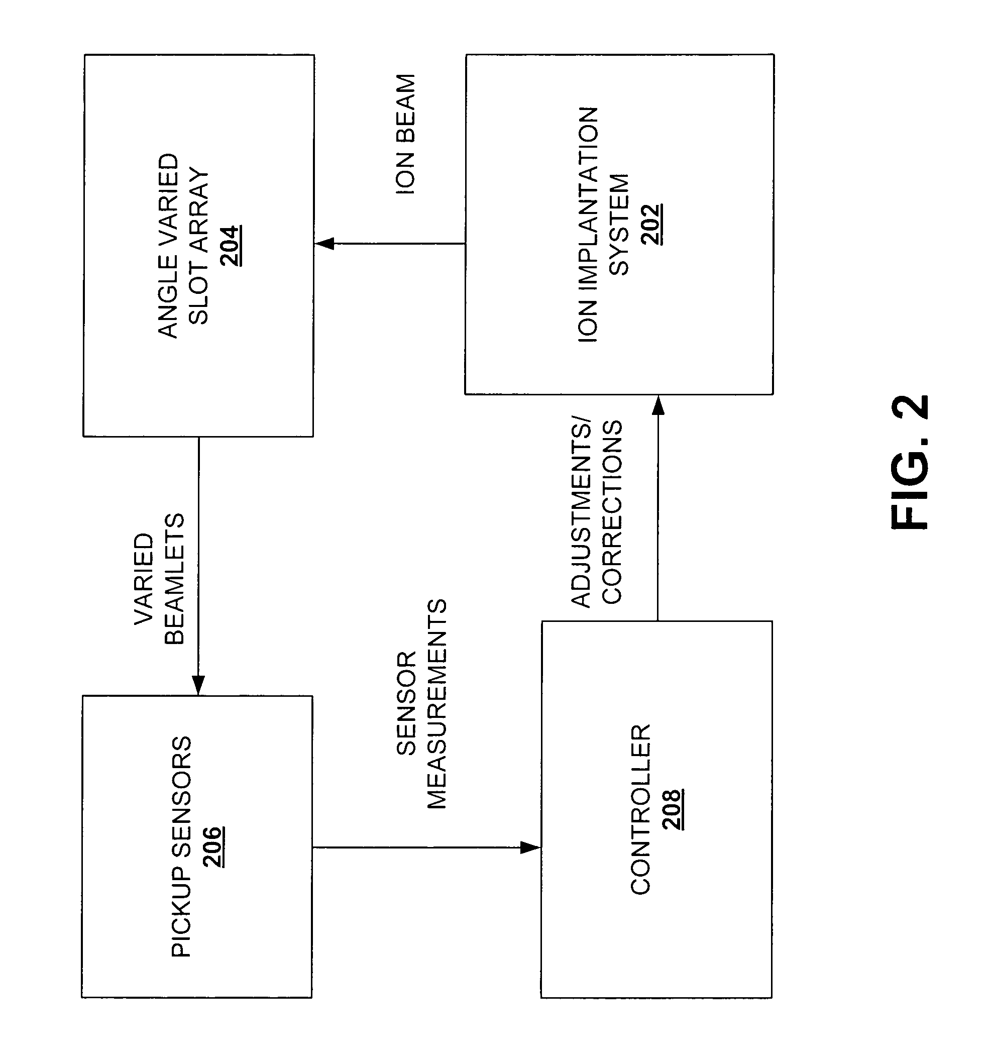
[0023]The present invention facilitates semiconductor device fabrication by detecting or measuring angle of incidence values for incident ion beams and optionally correcting angular errors before and / or during ion implantation procedures. The present invention employs varied angle slot arrays comprised of structures having a plurality of slots defined therein. The slot arrays select one or more beamlets from ion beams according to varied acceptance angles. Charge measurement sensors, such as pickup sensors, measure charge or beam current associated with each of the slots of the array. From these measurements and acceptance angles for each of the slots...


PUM


Abstract

An angle measurement system for measuring angles of incidence for ion beams during ion implantation includes a varied angle slot array and an array of charge measurement devices located downstream of the varied angle slot array. The varied angle slot array includes slots formed within a structure from an entrance surface to an exit surface. Each of the slots has a varied acceptance angle range. The array of charge measurement devices are individually associated with the slots and can measure charge or beam current for beamlets that pass through the slots. These measurements and the varied or different acceptance angle ranges can then be employed to determine a measured angle of incidence and / or angular content for an ion beam.

Description

FIELD OF INVENTION[0001]The present invention relates generally to semiconductor device fabrication and ion implantation, and more particularly, to calibrating, detecting and / or modifying an ion beam incident angle, directionally, during setup or in situ.BACKGROUND OF THE INVENTION[0002]Ion implantation is a physical process that is employed in semiconductor device fabrication to selectively implant dopant into semiconductor and / or wafer material. Thus, the act of implanting does not rely on a chemical interaction between a dopant and semiconductor material. For ion implantation, dopant atoms / molecules are ionized, accelerated, formed into a beam, analyzed, and swept across a wafer, or the wafer is swept through the beam. The dopant ions physically bombard the wafer, enter the surface and come to rest below the surface, at a depth related to their energy.[0003]An ion implantation system is a collection of sophisticated subsystems, each performing a specific action on the dopant ions...

Claims


Application Information

Patent Timeline
Patent Type & Authority Patents(United States)
IPC IPC(8): H05G2/00H05H1/00H05H1/24
CPCH01J37/244H01J37/304H01J37/3171H01J2237/24507H01J2237/24528H01J2237/24578H01J37/317H01L21/265
Inventor FREER, BRIAN S.
Owner AXCELIS TECHNOLOGIES
Why Eureka
Try Eureka