Semiconductor device comprising a photoelectric current amplifier

a semiconductor device and amplifier technology, applied in the field of semiconductor devices having photoelectric conversion elements, can solve the problems of reducing the voltage used for one level, reducing the resolving power, and expanding the range of output current, so as to achieve the effect of widening the detectable range of light intensity and narrowing the absolute value of output curren

Inactive Publication Date: 2009-02-03
SEMICON ENERGY LAB CO LTD
View PDF26 Cites 30 Cited by
  • Summary
  • Abstract
  • Description
  • Claims
  • Application Information

AI Technical Summary

Benefits of technology

[0016]According to a photoelectric conversion device of the present invention, a photoelectric current, which is generated from weak light by a photodiode, can be outputted with amplification by an amplifier circuit, and a photoelectric current, which is obtained by detecting light having illuminance of a certain level or more, can be outputted without amplification. Thus, an output current can be lowered once, the range of an absolute value of an output current can be narrowed, and a voltage value for one gray-scale can be increased. Accordingly, there is an advantage that a detectable range of light intensity is widened.

Problems solved by technology

With a conventional light sensor, weak light can be detected; however, when light from weak light to strong light is detected, there is a problem that a range of an output current is expanded and voltage used for one level is lowered.
Accordingly, resolving power is getting worse or an effect of noise is increased.

Method used


Image

  • Semiconductor device comprising a photoelectric current amplifier
  • Semiconductor device comprising a photoelectric current amplifier
  • Semiconductor device comprising a photoelectric current amplifier

Examples


embodiment 1

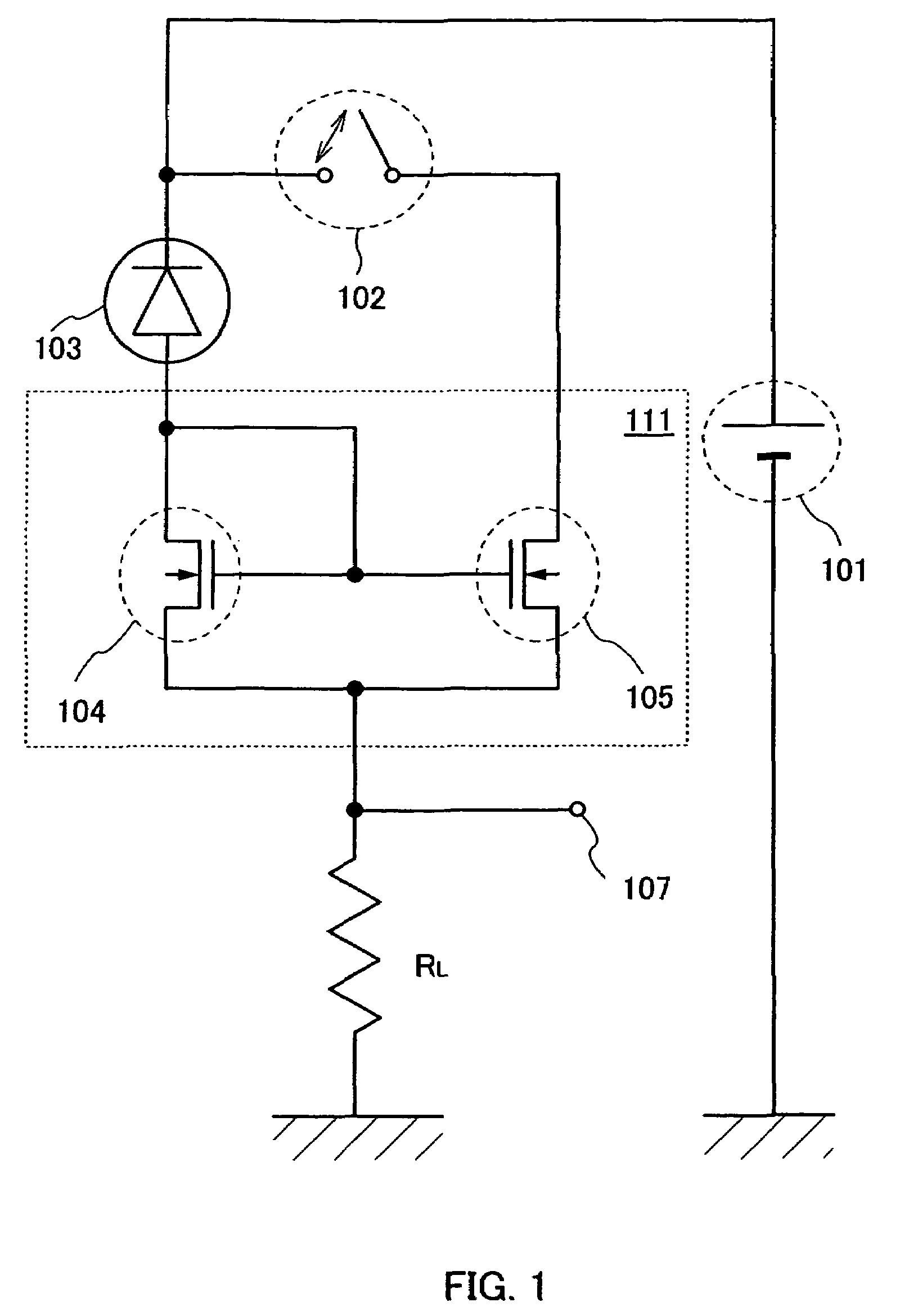
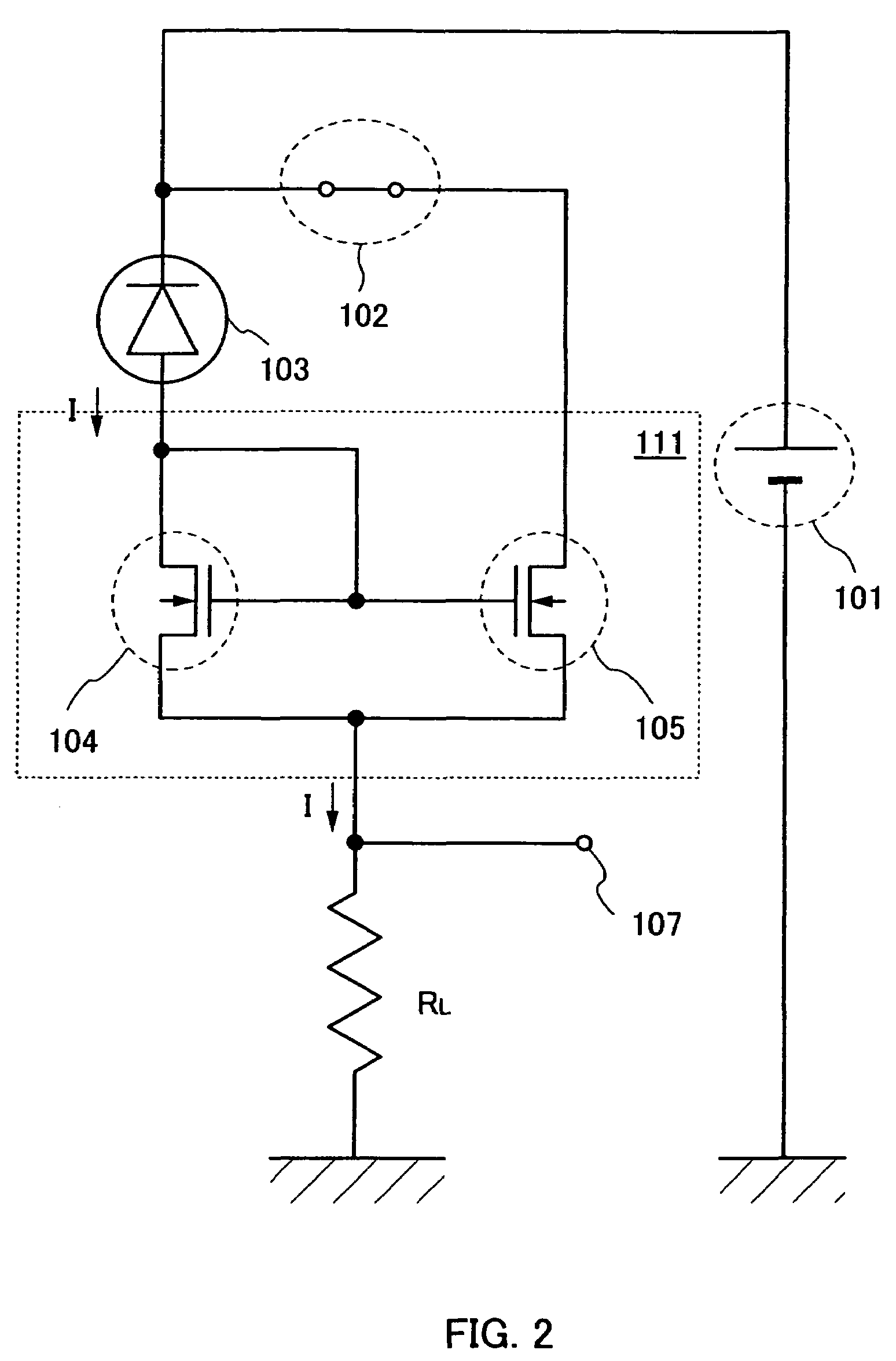
[0094]This embodiment will be explained with reference to FIGS. 6A and 6B, FIGS. 7A to 7D, FIGS. 8A to 8D, and FIGS. 9A to 9C. It is to be noted that the same reference numerals as those explained in “BEST MODE FOR CARRYING OUT THE INVENTION” are used.

[0095]First, an element is formed over a substrate (a first substrate 210). Here, AN 100 that is one of glass substrates is used as the substrate 210.

[0096]Subsequently, a silicon oxide film containing nitrogen which serves as a base insulating film 212 (100 nm thick) is formed by a plasma CVD method, and a semiconductor film such as an amorphous silicon film containing hydrogen (54 nm thick) is stacked thereover without being exposed to atmospheric air. In addition, a silicon oxide film, a silicon nitride film, and a silicon oxide film containing nitrogen may be stacked to form the base insulating film 212. For example, a silicon nitride film containing oxygen having a thickness of 50 nm, and further, a silicon oxide film containing n...

embodiment 2

[0146]In this embodiment, an example in which an amplifier circuit is made of a p-channel TFT will be explained with reference to FIG. 5 and FIGS. 10A and 10B. It is to be noted that the same portions as those in Embodiment Mode and Embodiment 1 are denoted by the same reference numerals, and the same portions may be formed on the basis of the manufacturing process described in Embodiment Mode and Embodiment 1.

[0147]In a case where an amplifier circuit, for example, a current mirror circuit 203 is made of p-channel TFTs 201 and 202, a p-type impurity, for example, boron (B) may be substituted for the impurity imparting one conductivity type to the island-like semiconductor region in Embodiment Mode and Embodiment 1.

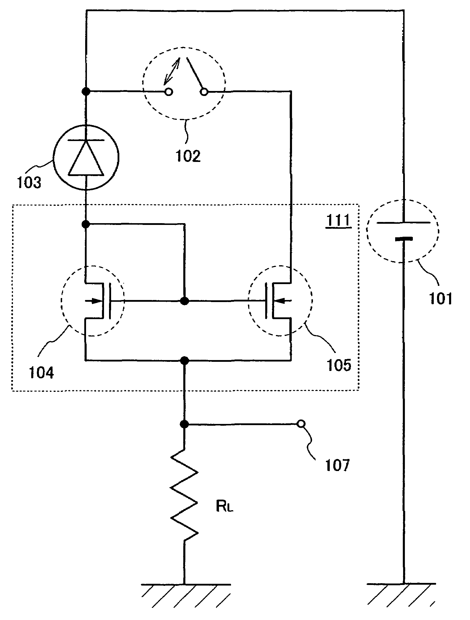
[0148]An equivalent circuit diagram of a light sensor of this embodiment in which the current mirror circuit 203 is made of the p-channel TFTs 201 and 202 is shown in FIG. 5, and cross-sectional views thereof are shown in FIGS. 10A and 10B.

[0149]In FIG. 5 and FIG. 10A, te...

embodiment 3

[0154]In this embodiment, an example of a light sensor in which an amplifier circuit is formed by using a bottom gate TFT and a manufacturing method thereof will be explained with reference to FIGS. 11A to 11E, FIGS. 12A to 12D, and FIGS. 13A and 13B. It is to be noted that the same portions as those in Embodiment Mode and Embodiments 1 and 2 are denoted by the same reference numerals.

[0155]First, a base insulating film 212 and a metal film 311 are formed over a substrate 210 (refer to FIG. 11A). As the metal film 311, in this embodiment, a film in which tantalum nitride (TaN) having a thickness of 30 nm and tungsten (W) having a thickness of 370 nm are stacked is used, for example.

[0156]In addition, as the metal film 311, as well as the above film, a single-layer film made of an element selected from titanium (Ti), tungsten (W), tantalum (Ta), molybdenum (Mo), neodymium (Nd), cobalt (Co), zirconium (Zr), zinc (Zn), ruthenium (Ru), rhodium (Rh), palladium (Pd), osmium (Os), iridium ...


PUM


Abstract

The present invention provides a photoelectric conversion device capable of detecting light from weak light to strong light and relates to a photoelectric conversion device having a photodiode having a photoelectric conversion layer; an amplifier circuit including a transistor; and a switch, where the photodiode and the amplifier circuit are electrically connected to each other by the switch when intensity of entering light is lower than predetermined intensity so that a photoelectric current is amplified by the amplifier circuit to be outputted, and the photodiode and part or all of the amplifier circuits are electrically disconnected by the switch so that a photoelectric current is reduced in an amplification factor to be outputted. According to such a photoelectric conversion device, light from weak light to strong light can be detected.

Description

TECHNICAL FIELD[0001]The present invention relates to a photoelectric conversion device and a semiconductor device having a photoelectric conversion element. Specifically, the present invention relates to a photoelectric conversion device formed by a thin film semiconductor element and a manufacturing method thereof. Moreover, the present invention relates to an electronic device using a photoelectric conversion device.BACKGROUND ART[0002]A number of photoelectric conversion devices generally used for detecting an electromagnetic wave are known, and for example, a photoelectric conversion device having sensitivity in ultra-violet rays to infrared rays is referred to as a light sensor in general. A light sensor having sensitivity in a visible radiation region with a wavelength of 400 to 700 nm is particularly referred to as a visible light sensor, and a large number of visible light sensors are used for devices which need illuminance adjustment or on / off control depending on human li...

Claims


Application Information

Patent Timeline
Patent Type & Authority Patents(United States)
IPC IPC(8): H03F3/08H03F3/04G01J1/42G01J1/44H01L31/10
CPCG01J1/44H01L31/102H04N5/2351H01L31/145H04N23/71H01L27/14H01L31/10
Inventor NISHI, KAZUOARAO, TATSUYAHIROSE, ATSUSHISUGAWARA, YUUSUKEKUSUMOTO, NAOTOYAMADA, DAIKITAKAHASHI, HIDEKAZU
Owner SEMICON ENERGY LAB CO LTD
Why Eureka
Try Eureka