Repair circuit and method of repairing defects in a semiconductor memory device

a semiconductor memory and repair circuit technology, applied in static storage, digital storage, instruments, etc., can solve the problems of memory cell defects, memory cell defects, and the layout of laser fuse circuits is more complicated than the one of the fuse circuits, so as to reduce the negative layout

Active Publication Date: 2009-02-03
SAMSUNG ELECTRONICS CO LTD
View PDF6 Cites 9 Cited by
  • Summary
  • Abstract
  • Description
  • Claims
  • Application Information

AI Technical Summary

Benefits of technology

[0010]In contrast, a repair circuit and method of repairing defects in a semiconductor memory device according to embodiments of the present invention significantly reduce the negative layout impact typically associated with conventional PPR techniques.

Problems solved by technology

However, defective memory cells are often formed within the main memory array due to variations in the manufacturing processes used to fabricate the memory cells as well as variations in electrical performance characteristics across a large number of memory cells.
There are many different types of memory cell defects, including row related defects and / or column related defects.
E-fuse circuits offer several performance advantages, but tend to be more complicated in their layout relative to laser fuse circuits.
Thus, conventional PPR techniques incorporating both the row and column repair circuits using e-fuse circuits occupy an unacceptably large layout area within the overall semiconductor memory device.

Method used


Image

  • Repair circuit and method of repairing defects in a semiconductor memory device
  • Repair circuit and method of repairing defects in a semiconductor memory device
  • Repair circuit and method of repairing defects in a semiconductor memory device

Examples


Embodiment Construction

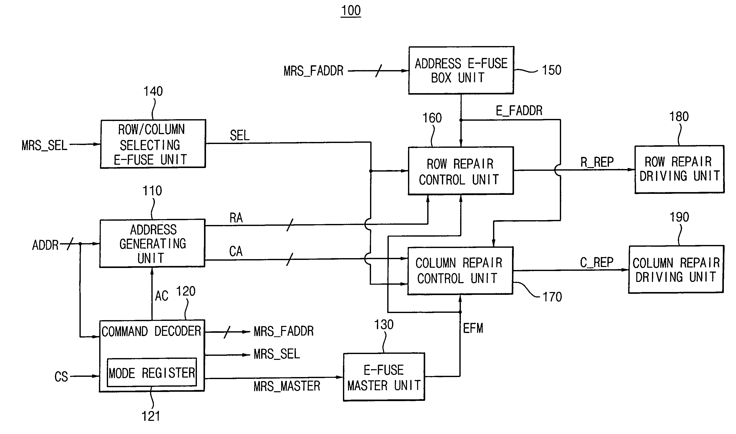
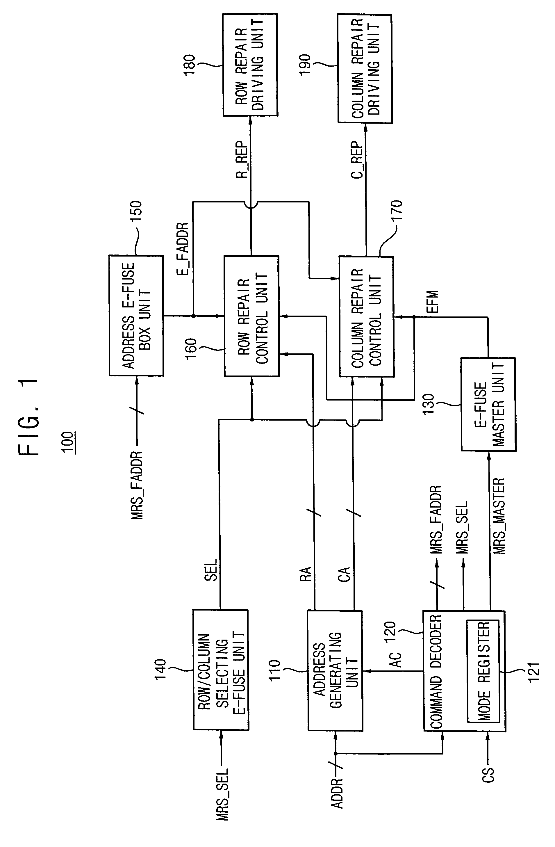
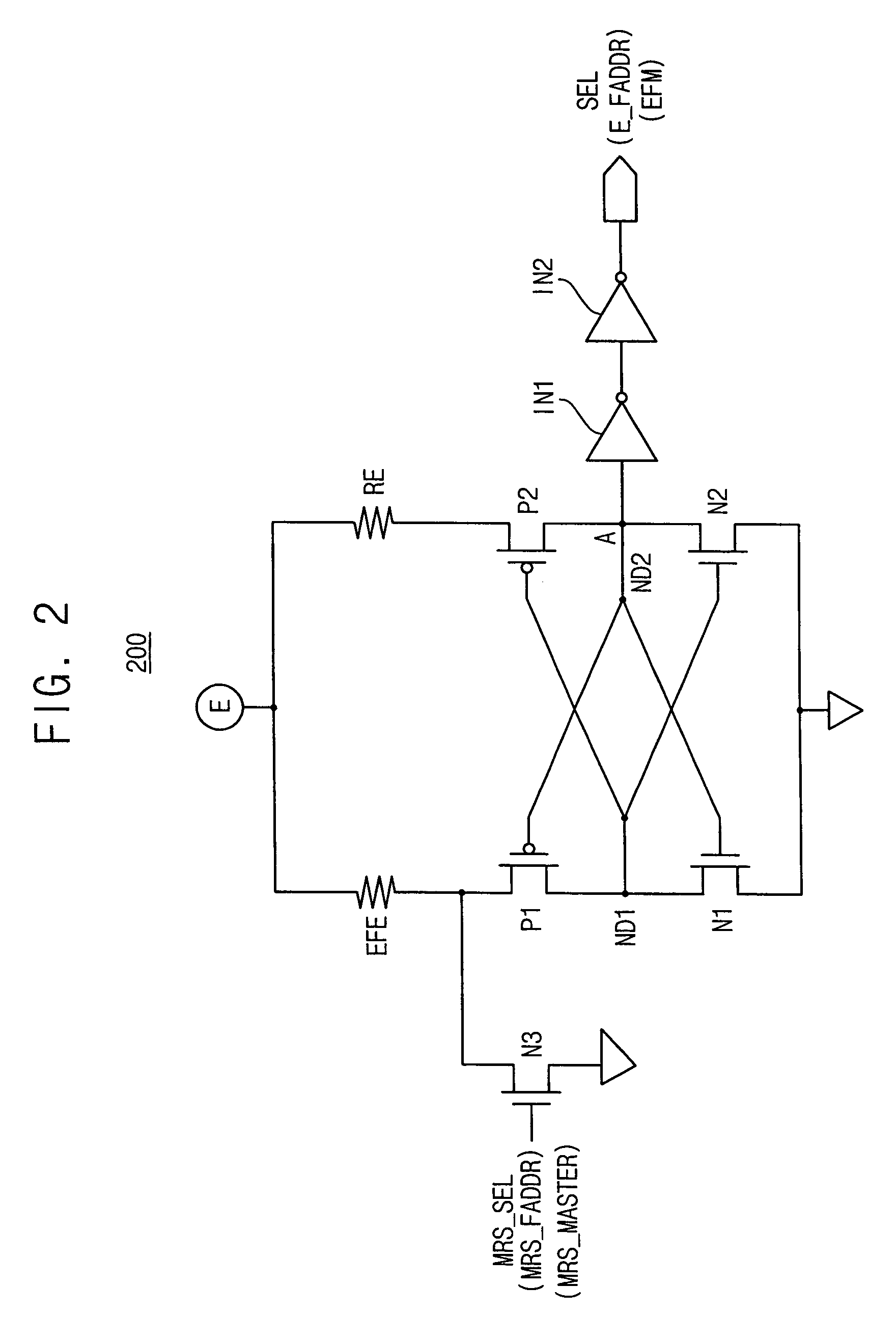
[0022]Embodiments of the present invention will now be described with reference to the accompanying drawings. The present invention may, however, be embodied in many different forms and should not be construed as being limited to only the illustrated embodiments. Rather, these embodiments are presented as teaching examples. Throughout the drawings and written description, like reference numerals refer to like or similar elements.

[0023]It will be understood that, although the terms first, second, etc. may be used herein to describe various elements, these elements should not be limited by these terms. These terms are used to distinguish one element from another. For example, a first element could be termed a second element, and, similarly, a second element could be termed a first element, without departing from the scope of the present invention. As used herein, the term “and / or” includes any and all combinations of one or more of the associated listed items.

[0024]It will be understo...


PUM


Abstract

A repair circuit and related method of repair are disclosed. In the repair circuit, row repair or column repair control units are selectively actuated to perform respective repair functions within a semiconductor memory device in relation to a commonly provided defective address. Both post-package defects and / or before package defects may be repaired in response to the defective address.

Description

BACKGROUND OF THE INVENTION[0001]1. Field of the Invention[0002]The present invention relates to semiconductor memory devices. More particularly, the present invention relates to a repair circuit and a method of repairing defects in a semiconductor memory device.[0003]This application claims priority under 35 USC § 119 to Korean Patent Application No. 2005-117258, filed on Dec. 3, 2005, the subject matter of which is incorporated herein in its entirety by reference.[0004]2. Description of the Related Art[0005]A semiconductor memory device generally includes a main memory array having a plurality of memory cells, and a redundant memory array having redundant memory cells adapted for use in the repair of defective memory cells in the main array. It is preferable that all memory cells of the main memory array operate normally. However, defective memory cells are often formed within the main memory array due to variations in the manufacturing processes used to fabricate the memory cells...

Claims


Application Information

Patent Timeline
Patent Type & Authority Patents(United States)
IPC IPC(8): G11C7/00
CPCG11C29/789G11C7/24G11C29/00
Inventor KIM, HYUNG-JIKJEONG, BYUNG-HOON
Owner SAMSUNG ELECTRONICS CO LTD
Why Eureka
Try Eureka