Discrete-time programmable-gain analog-to-digital converter (ADC) input circuit with multi-phase reference application

a technology of analog-to-digital converter and programmable-gain input circuit, which is applied in the direction of analogue/digital conversion, reversible analogue/digital converter, instruments, etc., can solve the problem that buffer circuits typically require considerable additional operating power

Active Publication Date: 2009-02-10
CIRRUS LOGIC INC
View PDF26 Cites 23 Cited by
  • Summary
  • Abstract
  • Description
  • Claims
  • Application Information

AI Technical Summary

Benefits of technology

[0008]The above stated objective of providing a low-power high-impedance discrete-time input circuit for an ADC that does not require buf...

Problems solved by technology

Furthermore, the buffer circuits typically...

Method used


Image

  • Discrete-time programmable-gain analog-to-digital converter (ADC) input circuit with multi-phase reference application
  • Discrete-time programmable-gain analog-to-digital converter (ADC) input circuit with multi-phase reference application
  • Discrete-time programmable-gain analog-to-digital converter (ADC) input circuit with multi-phase reference application

Examples


Embodiment Construction

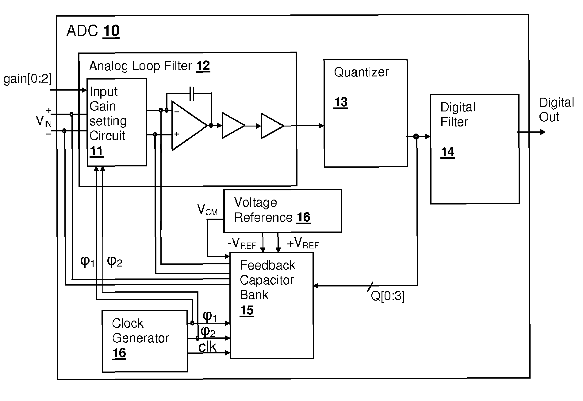
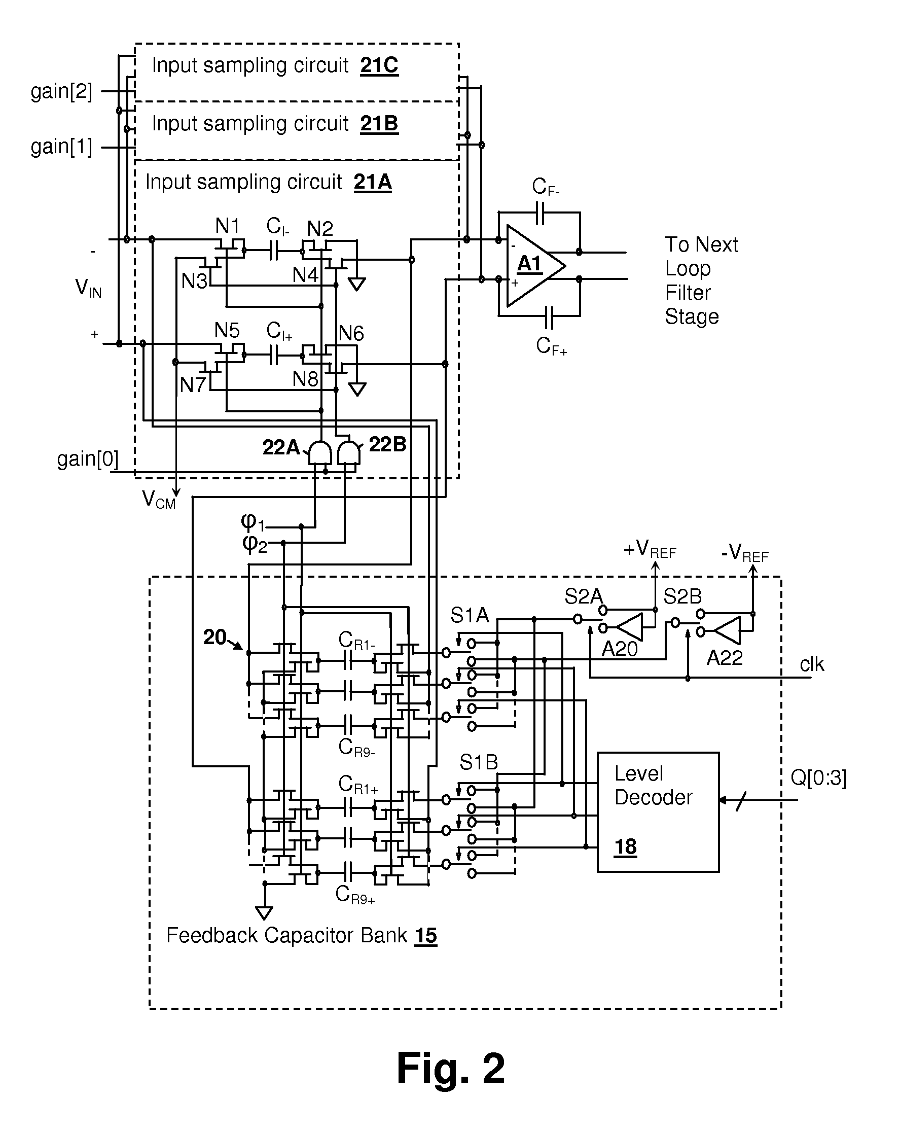
[0017]The present invention encompasses discrete-time sampling integrator circuits and delta-sigma modulator-based analog-to-digital (ADC) converter circuits, in which a high input impedance, for both common-mode and signal voltages, is provided by using the reference capacitor (or capacitor bank) that provides the quantizer-dependent feedback reference voltage value as an input sampling capacitor. At sampling time, the reference capacitor has a charge corresponding to the reference feedback voltage from a previous clock phase. There is no common-mode voltage on the reference capacitor from the previous clock phase, as during that clock phase, the reference feedback voltage is applied with respect to the reference common-mode voltage. Since the quantizer-dependent feedback reference voltage value matches the input signal at low frequencies, except for quantization error and noise, a very small signal current is drawn from the input(s), resulting in a high signal input impedance. Fur...


PUM


Abstract

A discrete-time programmable-gain analog-to-digital converter (ADC) input circuit with multi-phase reference application, provides a high input impedance level substantially independent of input capacitor size and input signal gain setting. An input voltage is sampled at the common mode voltage of the input, using one or more reference capacitor(s) that has been charged in a previous clock phase to the reference feedback voltage. The sampled input voltage is then applied in series with a quantizer-controlled reference voltage to the input of an integrator in a second clock phase. The summing mode of the integrator is maintained at the reference common-mode voltage. Since the charge pulled from the input voltage source is substantially determined only by the quantization error and input noise voltage, the circuit has a high signal input impedance. Since the input voltage source is sampled with respect to its common-mode voltage, the common-mode input impedance is also high.

Description

BACKGROUND OF THE INVENTION[0001]1. Field of the Invention[0002]The present invention relates generally to discrete-time input circuits, and more specifically, to a discrete-time analog-to-digital converter (ADC) input circuit having input signal and common-mode current nulling.[0003]2. Background of the Invention[0004]Measurement input circuits for ADCs must typically handle large common mode voltage differences between the input signal and the feedback reference voltage, especially in applications such as AC line power or DC measurement circuits and in test equipment such as digital voltmeters (DVMs). Even with the use of transformers or resistive dividers, the dynamic range needed for universal applicability typically requires one or more programmable gain stages to preserve signal to noise ratio (SNR) and a high input impedance buffer stage at the input to avoid loading the measured source, in particular where the source may have a large input voltage range requiring several gai...

Claims


Application Information

Patent Timeline
IPC IPC(8): H03M1/12
CPCH03M3/35H03M3/356H03M3/424H03M3/486
Inventor DRAKSHAPALLI, PRASHANTHPAULOS, JOHN
Owner CIRRUS LOGIC INC
Why Eureka
Try Eureka