Clock generator

a generator and clock technology, applied in the direction of generating/distributing signals, pulse techniques, instruments, etc., can solve the problems of skew generation between the reference clock signal and the frequency-divided clock signal, the difficulty of covering all states by performing operation inspection, and the decline of function, so as to achieve the effect of suppressing skew and improving timing convergen

Inactive Publication Date: 2009-02-17
PANASONIC SEMICON SOLUTIONS CO LTD
View PDF6 Cites 2 Cited by
  • Summary
  • Abstract
  • Description
  • Claims
  • Application Information

AI Technical Summary

Benefits of technology

[0007]In view of the above problem, it is therefore an object of the present invention to suppress skew between a reference clock signal and a frequency-divided clock signal caused by variation in the chip occurring in their transmission paths, thereby improving timing convergence.
[0009]In the inventive clock generator, the third circuit generates, from the first and second clock signals, the third clock signal which has the same period as that of the second clock signal and changes from the first logic level to the second logic level at the timing when the first clock signal changes from the first logic level to the second logic level. It is thus possible to suppress skew between the first clock signal and the third clock signal having the same period as the second clock signal obtained by dividing the frequency of the first clock signal.

Problems solved by technology

Also, in circuits which send and receive data asynchronously, it is difficult to cover all states by performing operation inspection.
In addition, redundant cycles are often needed in order to satisfy functional specifications, which causes decline in function.
However, a skew is generated between the reference clock signal and the frequency-divided clock signal, because those clock signals are transmitted through different paths and the like.
The occurrence of a skew may cause the semiconductor integrated circuit to malfunction.
Therefore, even if the conventional technique is applied to a semiconductor integrated circuit on which circuit operating at various frequencies are mounted, a skew occurring between a reference clock signal and a frequency-divided clock signal cannot be sufficiently suppressed just by forming the same circuit structures, and thus the problem that timing convergence is significantly worsened remains unsolved.

Method used


Image

  • Clock generator
  • Clock generator
  • Clock generator

Examples


first embodiment

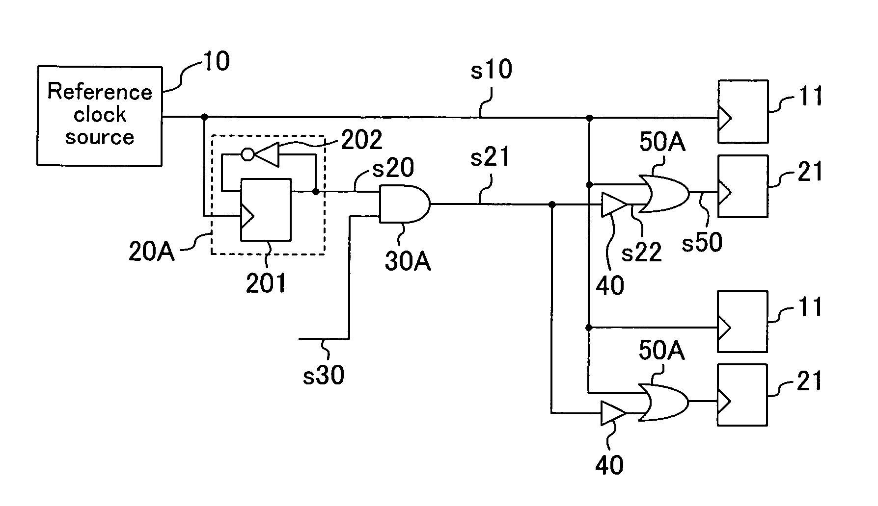
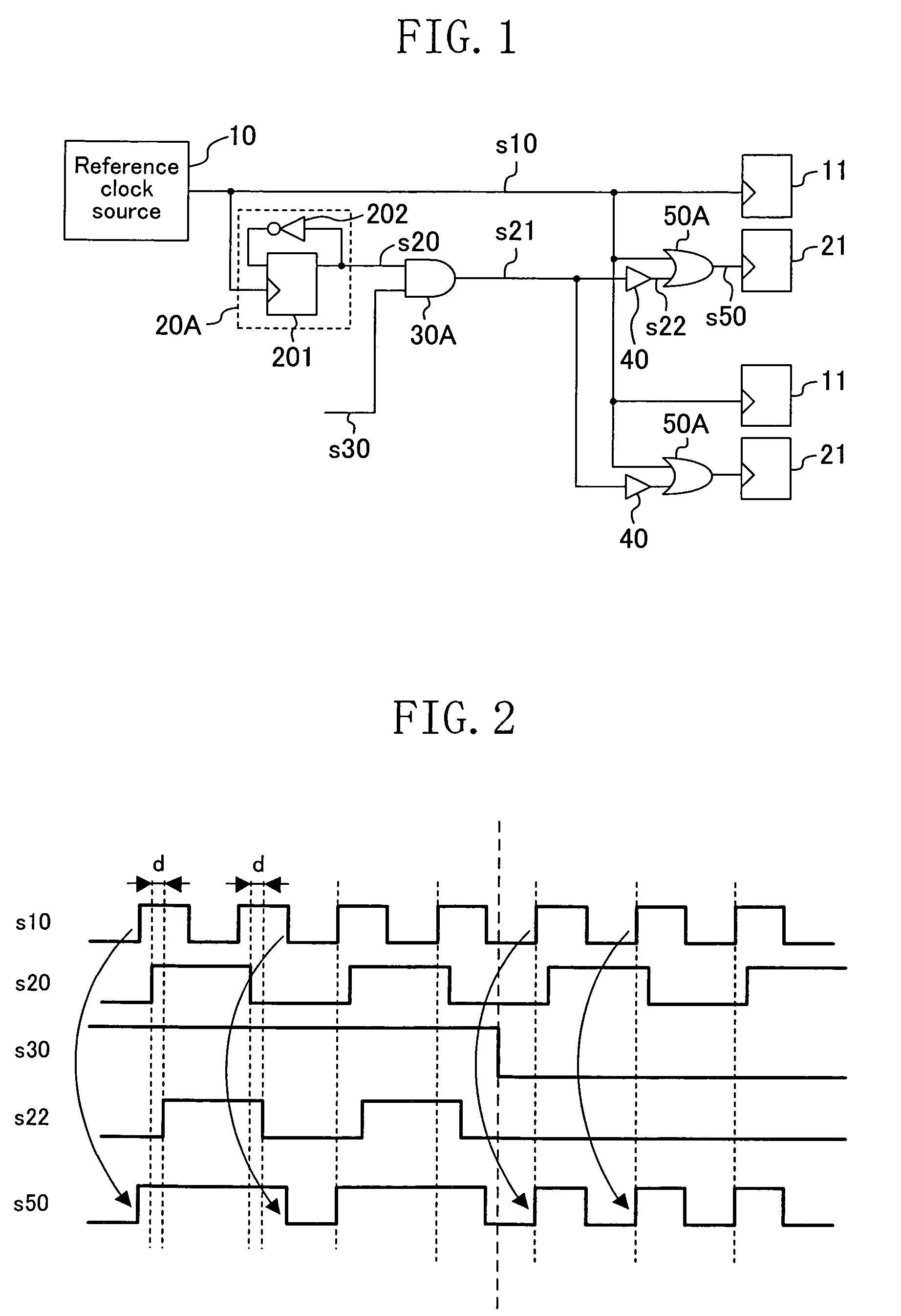
[0035]FIG. 1 illustrates the structure of a clock generator according to a first embodiment. This clock generator includes a reference clock source 10 as a first circuit, a frequency dividing circuit 20A as a second circuit, an AND gate 30A as a control circuit, delay circuits 40, and OR gates 50A as third circuits.

[0036]The reference clock source 10 generates a reference clock signal s10 as a first clock signal. The frequency dividing circuit 20A includes a flip-flop 201 and an inverter 202. The inverter 202 inverts the output signal of the flip-flop 201. The flip-flop 201 receives, as an input signal, the output signal of the inverter 202 and outputs a frequency-divided clock signal s20 as a second clock signal in synchronization with the rise of the reference clock signal s10. The AND gate 30A receives the frequency-divided clock signal s20 and a control signal s30 and performs an AND operation with respect to these signals to output a frequency-divided clock signal s21. The dela...

second embodiment

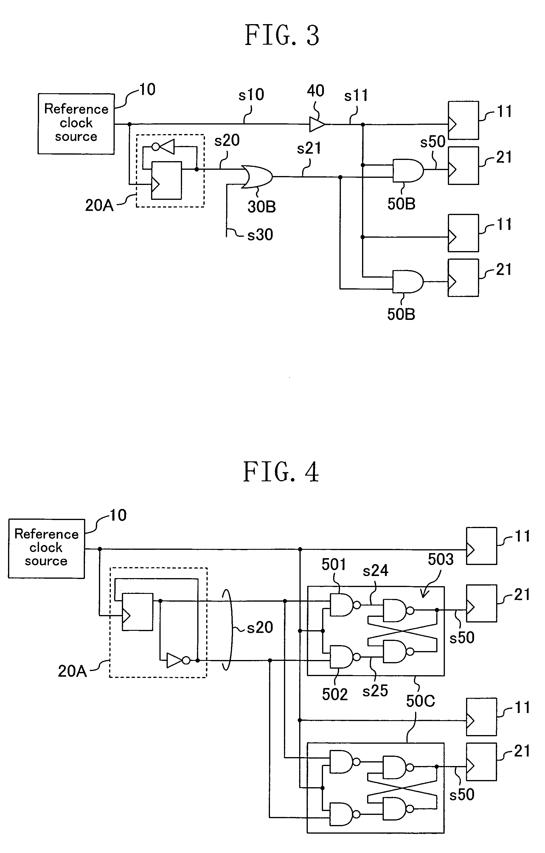
[0043]FIG. 4 illustrates the structure of a clock generator according to a second embodiment. This clock generator includes a reference clock source 10, a frequency dividing circuit 20A, and circuits 50C as third circuits. The frequency dividing circuit 20A outputs a frequency-divided clock signal s20 as a differential signal.

[0044]Each of the circuits 50C includes NAND gates 501 and 502 and an RS flip-flop 503. The NAND gate 501 receives a reference clock signal s10 and one side of the frequency-divided clock signal s20 output from the frequency dividing circuit 20A and outputs a frequency-divided clock signal s24. The NAND gate 502 receives the reference clock signal s10 and the other side of the frequency-divided clock signal s20 and outputs a frequency-divided clock signal s25. The RS flip-flop 503 receives, as input signals, the frequency-divided clock signals s24 and s25 output from the NAND gates 501 and 502.

[0045]FIG. 5 is a timing chart of the clock generator according to t...

third embodiment

[0047]FIG. 6 illustrates the structure of a clock generator according to a third embodiment. In this clock generator, the OR gate 30B in the clock generator shown in FIG. 3 is omitted, and three-input AND gates 50D are included in place of the AND gates 50B in the clock generator shown in FIG. 3. The AND gates 50D each receive an enable signal s31, as a control signal, in addition to a reference clock signal s11 and a frequency-divided clock signal s20 and perform an AND operation with respect to these signals to output a frequency-divided clock signal s50.

[0048]As described above, in this embodiment, it is possible to make the frequency-divided clock signal s50 switch between the valid and invalid states by using the enable signal s31. Also, the adoption of the three-input AND gate 50D permits this switching to be controlled without causing a particular increase in the circuit size.


PUM


Abstract

A clock generator includes a first circuit, a second circuit, and a third circuit. The first circuit generates a first clock signal. The second circuit divides the frequency of the first clock signal to generate a second clock signal. The third circuit generates a third clock signal from the first and second clock signals. The third clock signal has the same period as that of the second clock signal, and timing at which the third clock signal changes from a first logic level to a second logic level coincides with timing at which the first clock signal changes from a first logic level to a second logic level.

Description

CROSS-REFERENCE TO RELATED APPLICATION[0001]This application claims priority under 35 USC §119 to Japanese Patent Application No. 2006-3427 filed on Jan. 11, 2006, the entire contents of all of which are incorporated herein by reference.BACKGROUND OF THE INVENTION[0002]The present invention relates to a clock generator in a semiconductor integrated circuit including a plurality of circuits that operate in synchronization with clock signals of different frequencies.[0003]With reduction in the design rules for semiconductor integrated circuit fabrication processes, the number of transistors that can be integrated together on a single chip has been increasing dramatically. This enables the circuit to be multifunctional, thereby reducing the number of components therein and hence the costs thereof. That is, in order to reduce the number of design processes, existing design circuits are remounted. And circuits that need to operate at a specific frequency in conformity with a unified stan...

Claims


Application Information

Patent Timeline
Patent Type & Authority Patents(United States)
IPC IPC(8): G06F1/04
CPCG06F1/10
Inventor HAYAKAWA, NOBUHIRO
Owner PANASONIC SEMICON SOLUTIONS CO LTD
Why Eureka
Try Eureka