Comparator with low offset voltage

a technology of offset voltage and comparator, which is applied in the field of analog integrated circuits, can solve the problems of increasing cost, complicated manufacturing process, and complicated processing steps of embodiment, and achieve the effect of improving the offset voltag

Active Publication Date: 2009-03-10
HIMAX TECH LTD
View PDF6 Cites 20 Cited by
  • Summary
  • Abstract
  • Description
  • Claims
  • Application Information

AI Technical Summary

Benefits of technology

[0016]The present invention improves the offset voltage created by the process variations on the semiconductor devices, and in particular, the offset voltage of a comparator circuit.

Problems solved by technology

This means the embodiment involves more complex processing steps, i.e. expensive mixed-mode process.
However, this design requires the normal and enhancement transistors which can complicate the manufacturing process and increase the cost.
Moreover, this design also suffers the offset and mismatch problems.
As mentioned in this disclosure, the voltage error is primarily caused by current differences.
However, this design requires extra elements to overcome the variation in the primary pull-down devices.

Method used


Image

  • Comparator with low offset voltage
  • Comparator with low offset voltage
  • Comparator with low offset voltage

Examples


Embodiment Construction

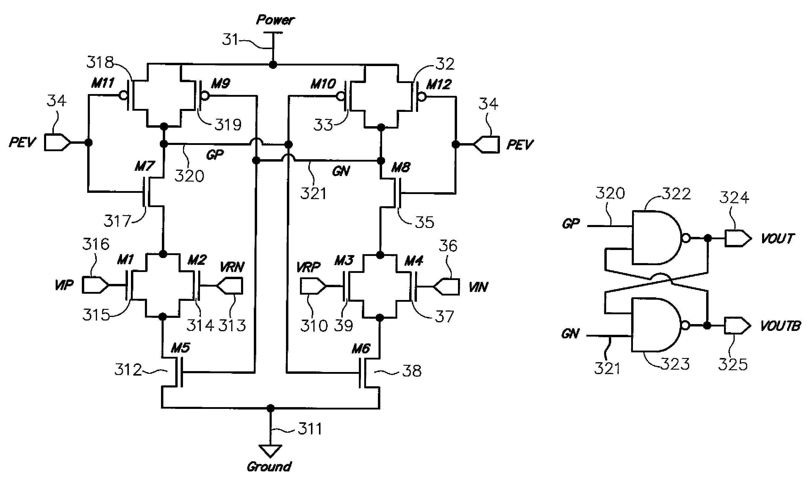
[0023]FIG. 3 illustrates a comparator with low offset voltage according to one embodiment of the invention. The comparator receives a first differential signal from an input signal VIP and a reference signal VRP, and receives a second differential signal from an input signal VIN and a reference signal VRN. The comparison result of the two differential signals may be represented by the signal on output terminals GP or GN, or by the signal VOUT or VOUTB.

[0024]The comparator includes (1) a positive feedback latch including two pairs of latch transistors, wherein one of the pairs includes PMOS transistor 319 and NMOS transistor 312, and the other pair includes PMOS transistor 33 and NMOS transistor 38, (2) a first pair of input transistors 315, 313, and (3) a second pair of input transistors 37, 39. The gates of the latch transistors 319 and 312 are coupled to the output terminal GN and the gates of the latch transistors 33 and 38 are coupled to the output terminal GP. The drain termina...


PUM


Abstract

A differential comparator is provided. The comparator receiving two differential signals and generating a comparison result represented by an output signal on one of two output terminals respectively on two current paths. The comparator comprises two pairs of latch transistors respectively disposed on the two current paths and two pairs of input transistors respectively disposed on the two current paths, wherein gates of the latch transistors on one of the current paths are commonly coupled to the output terminal between the latch transistors on the other current path, gates of the input transistors on one of the current paths respectively receives an input signal of one of the differential signals and a reference signal of the other differential signal and each of the input transistors is disposed between the output terminal and one of the latch transistors on the current path thereof.

Description

FIELD OF THE INVENTION[0001]The invention relates to analog integrated circuits, and in particular, to a comparator with low voltage offset.BACKGROUND OF THE INVENTION[0002]FIG. 1 illustrates a comparator that comprises several capacitors. Two pairs of voltages are provided. The first pair is VIP 115 and VIN 19 which represent the positive and negative inputs. The second pair is VRP 116 and VRN 18 which represent the positive and the negative reference inputs. Two capacitors 120 and 16 are used to receive input signals. An NMOS transistor 118, controlled by the phase I signal 117, is electrically connected to the VRP 116 and terminal 119 of the capacitor 120. An NMOS transistor 111, controlled by the phase I signal 17, is electrically connected to the VRN 18 and terminal 110 of the capacitor 16. A phase II signal 113 that controls an NMOS transistor 114 and an NMOS transistor 112 is also provided. The NMOS transistor 114 is electrically connected to the VIP 115 and terminal 119. The...

Claims


Application Information

Patent Timeline
Patent Type & Authority Patents(United States)
IPC IPC(8): H03K5/22
CPCH03K3/356113H03K3/356121
Inventor SU, TSUNG-YIHUANG, KUO-CHAN
Owner HIMAX TECH LTD
Why Eureka
Try Eureka