Dicing tape attaching apparatus and dicing tape attaching method

a technology of dicing tape and attaching apparatus, which is applied in the direction of mechanical control devices, instruments, semiconductor/solid-state device testing/measurement, etc., can solve the problems of internal distortion of wafers, and achieve the effect of preventing the formation of cuts, cracks and internal distortions

Inactive Publication Date: 2009-03-17
TOKYO SEIMITSU
View PDF20 Cites 8 Cited by
  • Summary
  • Abstract
  • Description
  • Claims
  • Application Information

AI Technical Summary

Benefits of technology

[0013]Specifically, in the first aspect, at the time of attaching the dicing tape, the wafer on the movable table and the mount frame on the fixed table can be made flush with each other by the height adjusting means. Thus, an unnecessary force, from the dicing tape attaching means, is not exerted on the edges of the wafer. As a result, the dicing tape can be attached on the mount frame and the wafer without forming cuts, cracks and internal distortions in the wafer.
[0035]Specifically, in the 12th aspect, the pressing force of the movable table is set in accordance with the covered distance of the dicing tape attaching means as calculated and, therefore, the surface pressure applied to the wafer is kept substantially and accurately equal over the whole wafer. As a result, the unnecessary force from the dicing tape attaching means is prevented from being exerted over the whole outer periphery of the wafer, thereby preventing the forming of cuts, cracks and internal distortions.

Problems solved by technology

Even in the case where cuts or cracks do not occur, internal distortions of the wafer is caused and may appear as cuts or cracks in the subsequent processes.

Method used


Image

  • Dicing tape attaching apparatus and dicing tape attaching method
  • Dicing tape attaching apparatus and dicing tape attaching method
  • Dicing tape attaching apparatus and dicing tape attaching method

Examples


Embodiment Construction

[0049]Embodiments of the invention are explained below with reference to the accompanying drawings. In the drawings, the same component members are designated by the same reference numerals, respectively. To facilitate the understanding, the scale of the drawings has been appropriately changed.

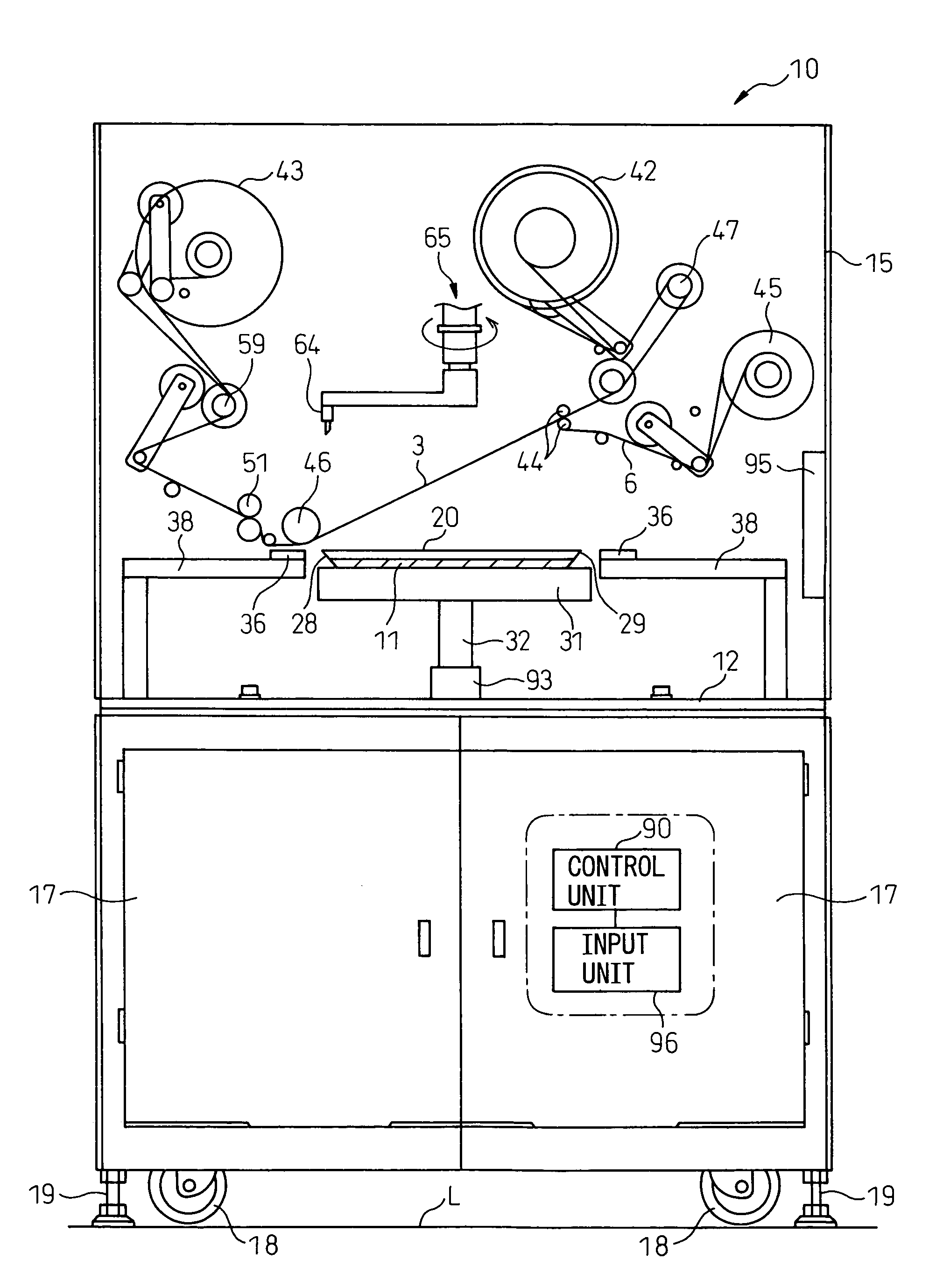
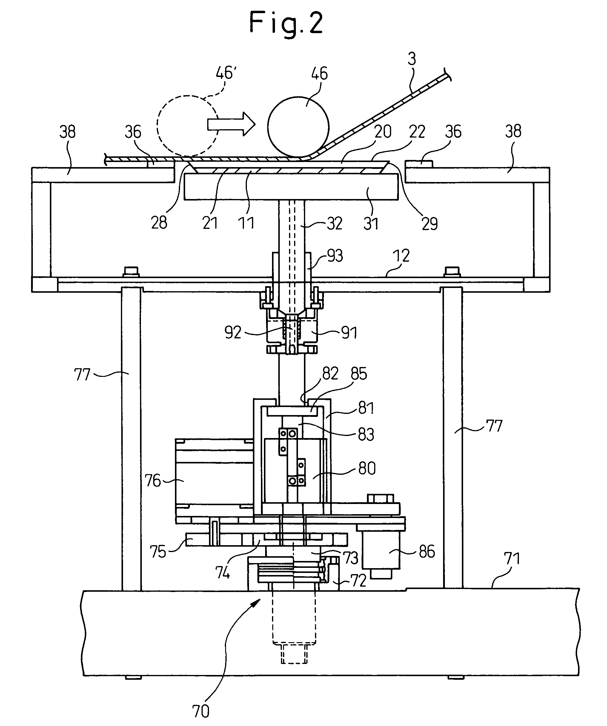
[0050]FIG. 1 is a sectional view schematically showing a dicing tape attaching apparatus according to this invention. The back surface of a wafer 20 supplied to a dicing tape attaching apparatus 10, as explained with reference to FIG. 7, is ground by back grinding to a chamfered portion 26 on the front surface thereof, and the thickness of the wafer 20 is not more than 100 micrometers. Also, as is well known, a surface protective film 11 for protecting the semiconductor elements is already attached on the front surface of the wafer 20.

[0051]The dicing tape attaching apparatus 10 shown in FIG. 1 includes a housing 15 containing therein a supply unit 42 for supplying a dicing tape 3 to be attach...


PUM

PropertyMeasurementUnit
thicknessaaaaaaaaaa
thicknessaaaaaaaaaa
heightaaaaaaaaaa

Abstract

A dicing tape attaching apparatus (10) comprises a fixed table (38) for supporting a mount frame (36), a movable table (31) for supporting a wafer (20) with the reverse surface thereof ground, and a height adjusting unit (70) such as a screw jack for adjusting the height of the movable table. When the dicing tape (3) is attached on the mount frame and the wafer, the height adjusting unit such as the screw jack so operates that the height of the dicing tape attaching surface of the wafer supported on the movable table coincides with the height of the upper surface of the mount frame supported on the fixed table. As a result, the wafer is prevented from forming cuts, cracks and internal distortions.

Description

CROSS-REFERENCE TO RELATED APPLICATION[0001]This application claims priority of Japanese Application Number 2005-340145, filed on Nov. 25, 2005.BACKGROUND OF THE INVENTION[0002]1. Field of the Invention[0003]This invention relates to a dicing tape attaching method, for attaching a dicing tape on the back surface of a wafer, and to a dicing tape attaching apparatus for carrying out the method.[0004]2. Description of the Related Art[0005]In the semiconductor fabrication field, wafers have increased in size every year, on the one hand, and, in order to increase the mounting density, the thickness of the wafer has been reduced. The thickness of the wafer is reduced by a back grind process which grinds the back surface of the semiconductor wafer. In the back grind process, a surface protective tape is attached on the front surface of the wafer to protect the semiconductor elements formed on the front surface.[0006]FIG. 7 is an enlarged sectional view of a circular wafer with a surface pr...

Claims


Application Information

Patent Timeline
Patent Type & Authority Patents(United States)
IPC IPC(8): B32B41/00
CPCH01L21/67132H01L21/08
Inventor AMETANI, MINORU
Owner TOKYO SEIMITSU
Why Eureka
Try Eureka