
Method and mechanism for implementing DFM aware cells for an electronic design

Inactive Publication Date: 2009-03-17
CADENCE DESIGN SYST INC
View PDF4 Cites 30 Cited by
  • Summary
  • Abstract
  • Description
  • Claims
  • Application Information

AI Technical Summary

Benefits of technology

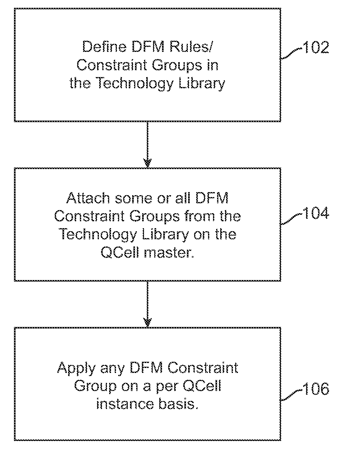
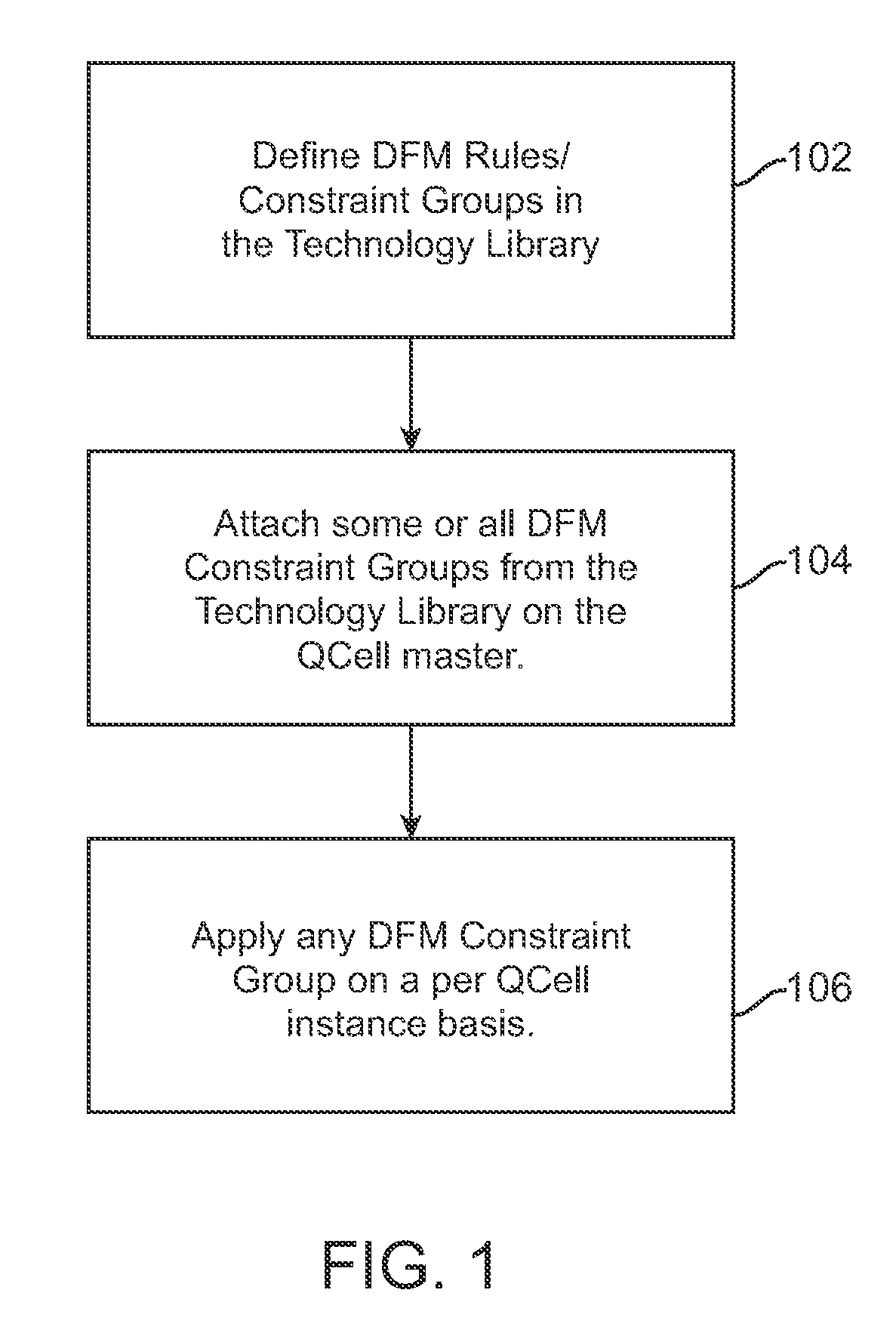
[0008]To address these issues (among others), embodiments of the present invention provide an improved method, system, computer program product, and electronic design structures which provides the flexibility to IC designers to be able to relax the design rules to increase the yield and improve the layout productivity. In some embodiments, automated interactive aids and batch tools are provided which can assist in optimizing the final layouts for yield at the initial placement and / or routing stages for optimizing yield. Provided in some embodiments are automated capability to layout designers at the mos devices level to configure mos devices as per different DFY recommendations from the foundry without negative effects on the overall chip area (or cell size). The design rules may be relaxed selectively on an instance basis and wherever possible or desirable.

Problems solved by technology

Therefore, strict application of the rules may actually decrease yield for manufacturing of the IC device if portions of the rules are stricter than needed for every given component on an IC.
The emerging state of nanometer semiconductor production demands that designers take yield into consideration up front, rather than leaving it as an expensive and time-consuming afterthought.
One problem with this approach is that the user can lose backannotation of the impacted devices with their corresponding schematics.
Since the parameterized devices get flattened, it creates problems in Engineering Change Order (“ECO”) flow (e.g., using Update Layout Parameters) or while picking any later updates from the schematic automatically.
A problem with this approach is that it can cause great difficulties and costs to maintain different masters of the same device just for having different DFM rules.

Method used


Image

  • Method and mechanism for implementing DFM aware cells for an electronic design
  • Method and mechanism for implementing DFM aware cells for an electronic design
  • Method and mechanism for implementing DFM aware cells for an electronic design

Examples


examples

[0063]The present example(s) show the changes in device geometry when the DFM rules are applied to the QCell instance. FIG. 6 shows the geometry of a QCell Instance without application of any DFM Rule. FIG. 7 shows the changed geometry when the value of Poly to Contact Spacing DFM rule is set to highYield, i.e., increased. The new increased value of Poly to Contact spacing is being reflected in the device geometry.

[0064]FIG. 8 shows the changed geometry of the QCell instance when both of the Poly to Contact Spacing as well as Active Enclosure of Contact are set to highYield. This automatically updates the number of contacts within the same device width and metal shape, depending on the application of new Active Enclosure of Contact which is slightly mordthan its corresponding DRC value.

DFM Intelligent QCells' Position in the Design Flow

[0065]In some embodiments, the inventive DFM concepts can be used for individual Qcell MOS devices which are the building blocks of any complex desig...


PUM


Abstract

An improved method, system, computer program product, and electronic design structures which provides the flexibility to IC designers to be able to relax the design rules to increase the yield and improve the layout productivity is disclosed. In some disclosed approaches, automated interactive aids and batch tools are provided which can assist in optimizing the final layouts for yield at the initial placement and / or routing stages for optimizing yield. Provided in some disclosed approaches are automated capability to layout designers at the mos devices level to configure mos devices as per different DFY recommendations from the foundry without negative effects on the overall chip area (or cell size). The design rules may be relaxed selectively on an instance basis and wherever possible or desirable.

Description

CROSS-REFERENCE TO RELATED APPLICATION[0001]The present application claims the benefit of U.S. Provisional Application Ser. No. 60 / 704,192, filed on Jul. 28, 2005, which is hereby incorporated by reference in its entirety.BACKGROUND AND SUMMARY[0002]The invention relates to technology for implementing electronic design automation (“EDA”) tools and electronic designs using EDA tools.[0003]An IC is a small electronic device typically formed from semiconductor material. Each IC contains a large number of electronic components, e.g., transistors, that are wired together to create a self-contained circuit device. The components and wiring on the IC are materialized as a set of geometric shapes that are placed and routed on the chip material. During placement, the location and positioning of each geometric shape corresponding to an IC component are identified on the IC layers. During routing, a set of routes are identified to tie together the geometric shapes for the electronic components...

Claims


Application Information

Patent Timeline
IPC IPC(8): G06F17/50G06F9/45
CPCG06F17/5081G06F2217/64G06F30/398G06F2115/06
Inventor ARORA, RAJANSISODIA, UMESHJAIN, ANURAG
Owner CADENCE DESIGN SYST INC
Learn More