
Fabrication of semiconductor devices

a technology of semiconductor devices and fabrication methods, applied in semiconductor devices, semiconductor/solid-state device details, electrical apparatus, etc., can solve the problems of increasing fabrication costs, microelectronic device fabrication costs, and use of expensive patterned masks

Inactive Publication Date: 2009-03-24
WODEN TECH INC
View PDF31 Cites 5 Cited by
  • Summary
  • Abstract
  • Description
  • Claims
  • Application Information

AI Technical Summary

Benefits of technology

This approach reduces fabrication costs by avoiding expensive lithography and mask requirements, enables the use of multiple material layers, and allows for the creation of complex microelectronic devices without the limitations of single-layer processes, such as dual-damascene, thereby enhancing device functionality and efficiency.

Problems solved by technology

A substantial portion of the cost of microelectronic device fabrication is attributable to the capital cost of lithography equipment.
Photolithography requires the use of expensive patterned masks.
The cost of fabrication increases as the device geometry becomes more complex and the feature size diminishes.
This process is very slow because the features are typically drawn sequentially by a single electron beam.
As a result, this process is limited in terms of the circuitry it can be used to create.

Method used


Image

  • Fabrication of semiconductor devices
  • Fabrication of semiconductor devices
  • Fabrication of semiconductor devices

Examples


Embodiment Construction

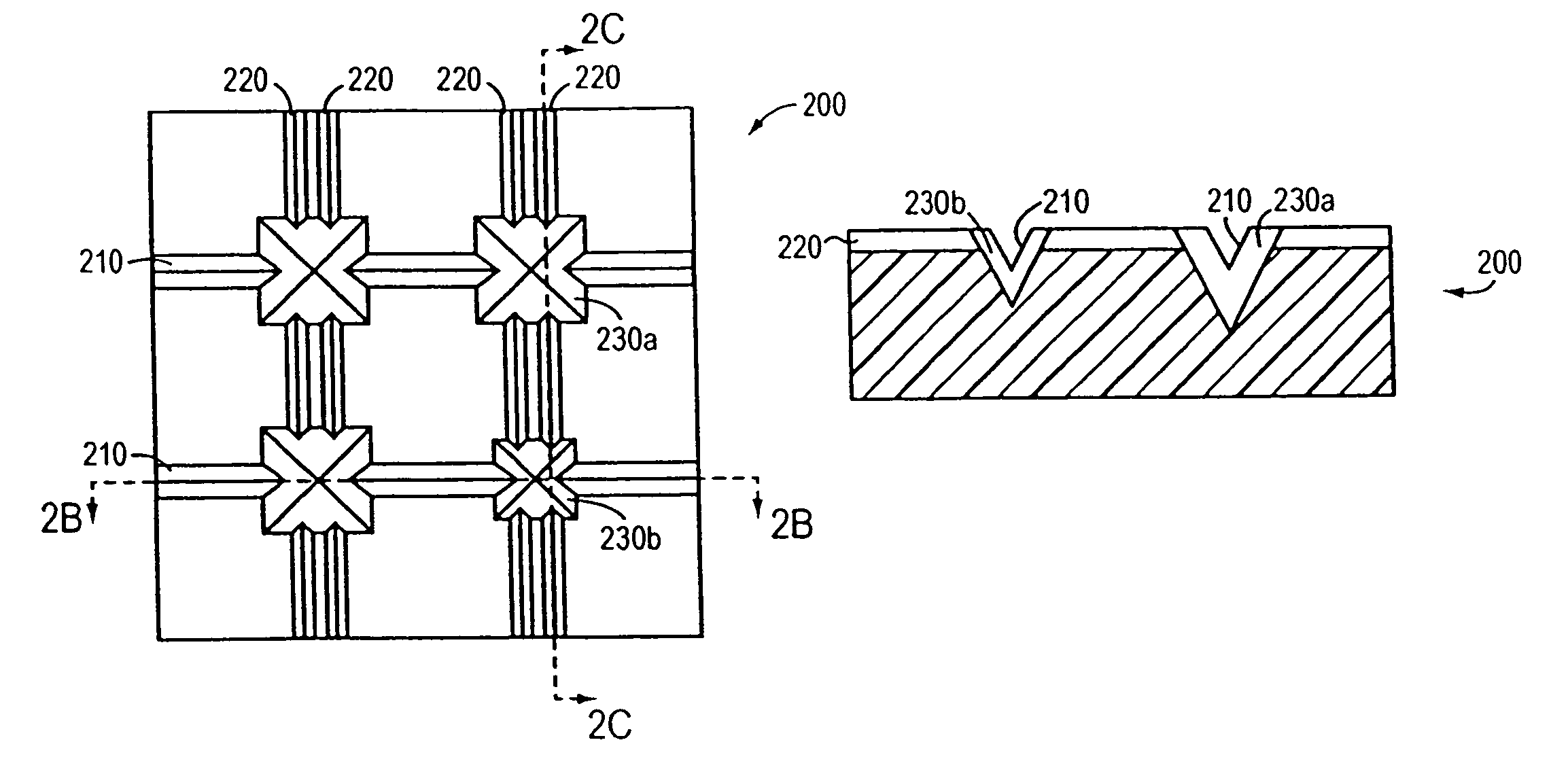
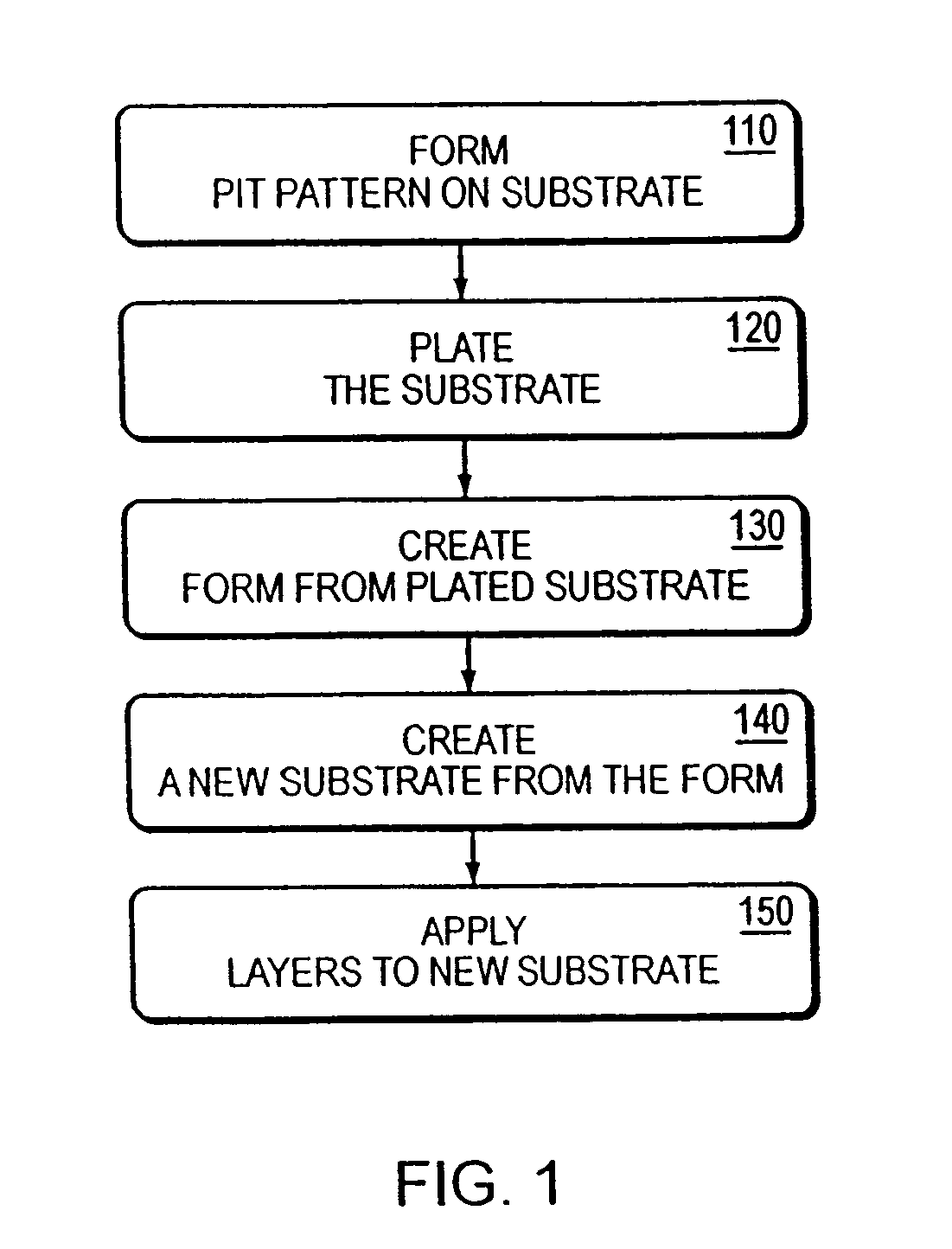
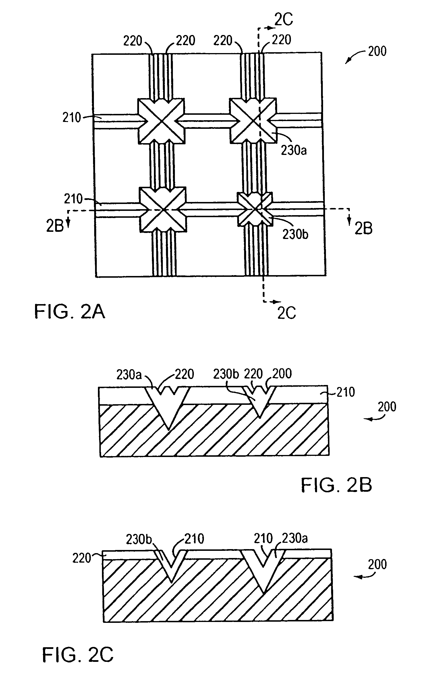
[0036]Devices in accordance with the invention may be fabricated using a molding process, which obviates the need to etch a recessed pattern into each substrate. Such a process is illustrated in FIG. 1. With reference to FIG. 1, a “master” substrate is etched with the recessed pattern (step 110). This master substrate is then plated (e.g., nickel sputtered) (step 120) in a manner similar to conventional CD and DVD fabrication. The metal-plated master is electroformed to create a form having a raised topology complementary to the recessed pattern of the substrate (step 130). Electroforming is the process of replicating the surface of a master by plating directly over it. A plating material is applied until the desired thickness is achieved. The remaining cavity block is back-filled for strength and then mounted in a frame. In other words, the recesses become raised features. Variations on the electroforming of the master copy could include depositing on that master copy material inte...


PUM


Abstract

Fabrication of microelectronic devices is accomplished using a substrate having a recessed pattern. In one approach, a master form is used to replicate a substrate having a pit pattern. In another approach, the substrate is produced by etching. A series of stacked layers having desired electrical characteristics is applied to the substrate and planarized in a manner that creates electrical devices and connections therebetween. The microelectronic devices can include a series of row and columns and are used to store data at their intersection.

Description

CROSS-REFERENCE TO RELATED APPLICATIONS[0001]This application claims the benefit of and priority to U.S. patent application Ser. No. 10 / 459,699, filed Jun. 11, 2003, now U.S. Pat. No. 7,183,206, which is a continuation of U.S. patent application Ser. No. 09 / 965,622, filed Sep. 27, 2001, now U.S. Pat. No. 6,586,327, which claims the benefits of U.S. Provisional Application No. 60 / 235,853, filed on Sep. 27, 2000; the entire disclosures of all three applications are hereby incorporated by reference.FIELD OF THE INVENTION[0002]The invention relates to microelectronic devices and there fabrication.BACKGROUND OF THE INVENTION[0003]A substantial portion of the cost of microelectronic device fabrication is attributable to the capital cost of lithography equipment. Such equipment produces integrated circuits by drawing patterns on a substrate using commonly known methods, such as photolithography, e-beam lithography, as well as many others. Photolithography requires the use of expensive patt...

Claims


Application Information

Patent Timeline
Patent Type & Authority Patents(United States)
IPC IPC(8): H01L21/44H01L29/872H01L21/3205H01L21/762H01L21/77H01L21/84H01L23/52H01L27/10H01L27/105H01L27/12H01L29/47
CPCH01L21/76229H01L21/76232H01L21/84H01L27/101H01L27/1203H01L27/1214H10B20/25
Inventor SHEPARD, DANIEL R.
Owner WODEN TECH INC
Learn More