Preparation of photomask blank and photomask

a technology of photomask and photomask, which is applied in the field of preparation can solve the problems of imposing detrimental effects on the manufacturing yield of products, narrow process margins, and lower stability, and achieve the effect of suppressing any change in phase shift of phase shifter films and improving the chemical resistance of photomask blanks and photomasks

Active Publication Date: 2009-04-07
SHIN ETSU CHEM IND CO LTD
View PDF4 Cites 8 Cited by
  • Summary
  • Abstract
  • Description
  • Claims
  • Application Information

AI Technical Summary

Benefits of technology

[0011]The inventor has discovered that in the preparation of a photomask blank having a light-absorbing film formed on a transparent substrate, the light-absorbing film after its formation is irradiated with light from a flash lamp at a predetermined energy density, whereby the film stress of the photomask blank can be controlled. By irradiating the light-absorbing film with light from a flash lamp, the stress in the light-absorbing film is optimized so as to minimize the warp of the photomask blank. Thus, a photomask resulting from this photomask blank enables pattern exposure at a finer feature size and at a higher precision.
[0012]More specifically, in the method of making a photomask blank having a light-absorbing film on a transparent substrate, once a light-absorbing film is formed on a transparent substrate, the light-absorbing film having a certain stress produced therein is irradiated with light from a flash lamp (1) at an energy density of 3 to 40 J / cm2; or (2) at such an energy density that the stress in the light-absorbing film becomes −300 to 300 MPa in compression stress as a result of light exposure; or (3) at an energy density in a range of ±5 J / cm2 relative to the central value equal to the energy density at which the stress in the light-absorbing film is 0 MPa as a result of light exposure. The controlled flashing light irradiation enables to reduce the film stress to nearly zero (a warpage of not more than about 0.1 μm). In addition, the stress in the light-absorbing film is controlled while taking into account the partial release of the film stress by patterning during the preparation of a photomask from the photomask blank. The thus obtained photomask is endowed with optimum flatness.
[0022]The present invention ensures the preparation of a photomask blank and a photomask, both having a warpage controlled to a predetermined or optimum range. At the same time, the invention is successful in improving the chemical resistance of the photomask blank and photomask, and especially in suppressing any change in phase shift of the phase shifter film by alkali treatment.

Problems solved by technology

The reduction of exposure wavelength improves the resolution, but reduces the depth of focus (DOF), which leads to a narrower process margin and lower stability, imposing detrimental impact on the manufacturing yield of products.
The resulting photomask blank thus suffers warp due to the film stress.

Method used


Image

  • Preparation of photomask blank and photomask
  • Preparation of photomask blank and photomask

Examples


example

[0059]Examples of the invention are given below by way of illustration and not by way of limitation.

examples 1 to 5

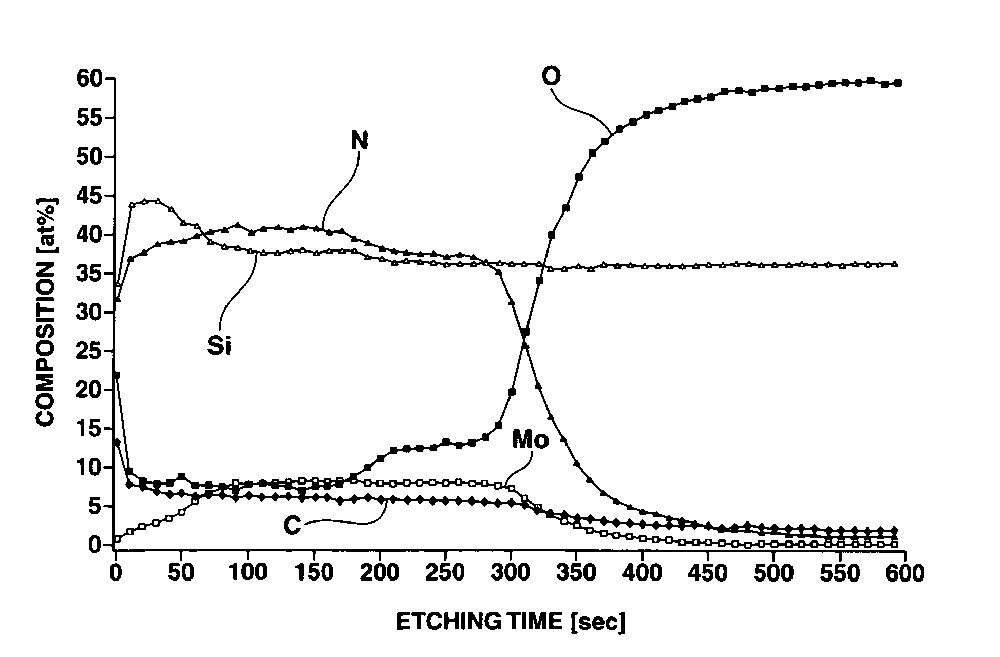
[0060]A halftone phase shift film of MoSiON was deposited on a square quartz substrate of 6 inches on one side by reactive DC sputtering of a MoSi target such that at the end of flash lamp irradiation, the film might have a phase shift of 180° relative to exposure light (ArF excimer laser: 193 nm), a transmittance of 6% with respect to exposure light (provided that the bare substrate had a transmittance of 100% with respect to exposure light), and a thickness of about 700 angstroms.

[0061]The substrate having the halftone phase shift film deposited thereon was heated at a temperature of 80° C., and then irradiated with light from a xenon flash lamp at an energy density reported in Table 1. The flash lamp was operated to produce flashes of light having a duration of about 1 to 10 msec by controlling the voltage. The irradiation included a single flash of light (the same being true in the following examples). The stress in the film before and after the flash lamp irradiation was determ...

example 6

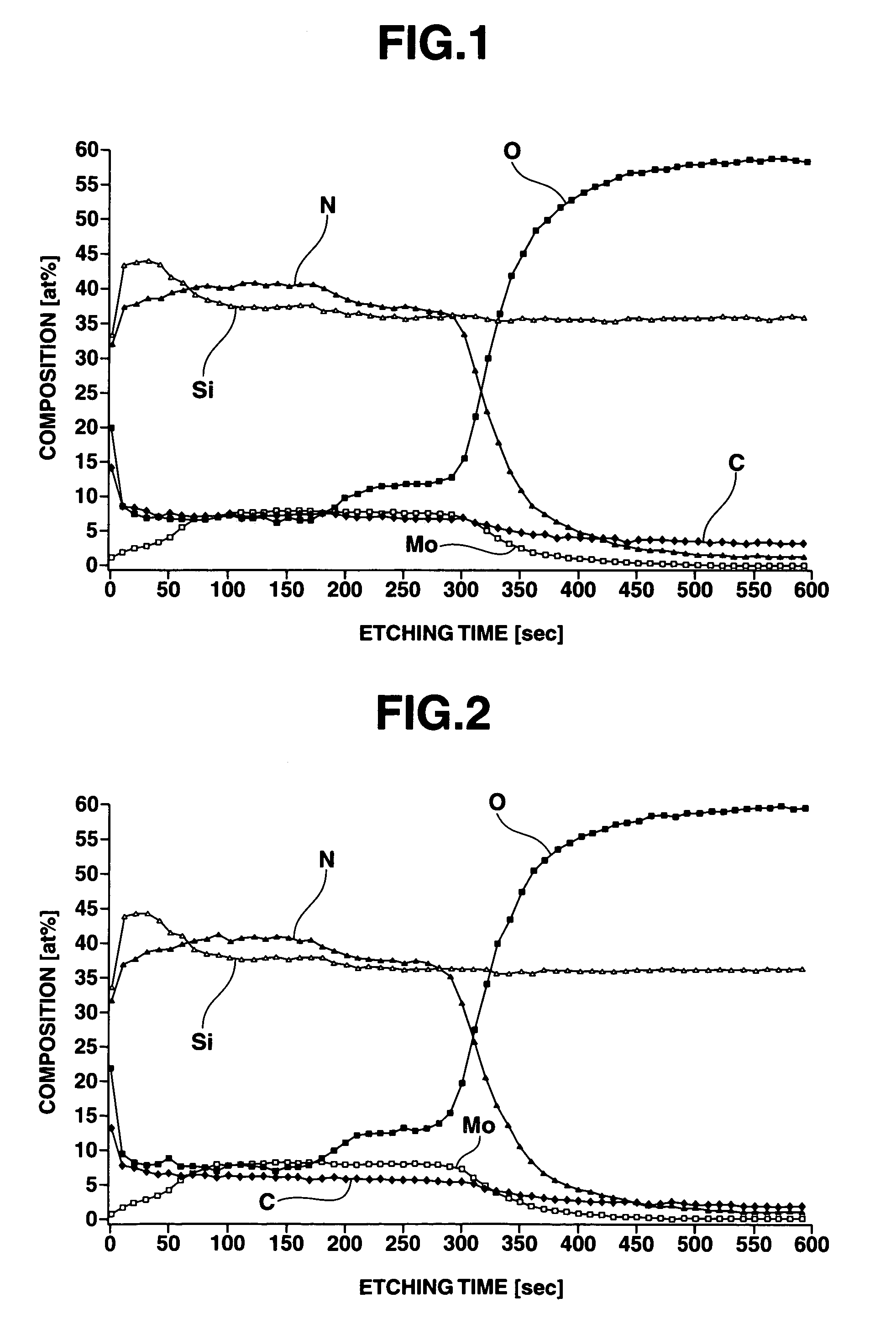
[0077]A halftone phase shift film of MoSiON was deposited on a substrate as in Example 1 except that the transmittance was set at 20%, and then irradiated with flash lamp light as in Example 1 except that the flash lamp irradiation was made at the energy density reported in Table 4. The film stress before and after the irradiation was determined, with the results shown in Table 4.


PUM

PropertyMeasurementUnit
energy densityaaaaaaaaaa
transmittanceaaaaaaaaaa

Abstract

A photomask blank is prepared by forming a light-absorbing film on a transparent substrate, and irradiating the light-absorbing film with light from a flash lamp at an energy density of 3 to 40 J / cm2. A photomask is prepared by forming a resist pattern on the photomask blank by photolithography, etching away those portions of the light-absorbing film which are not covered with the resist pattern, and removing the resist.

Description

CROSS-REFERENCE TO RELATED APPLICATION[0001]This non-provisional application claims priority under 35 U.S.C. §119(a) on Patent Application No. 2004-147403 filed in Japan on May 18, 2004, the entire contents of which are hereby incorporated by reference.TECHNICAL FIELD[0002]This invention relates to a method for preparing a photomask blank and a photomask for use in the microprocessing of semiconductor integrated circuits, color filters for charge-coupled device (CCD) and liquid crystal display (LCD), magnetic heads and the like.BACKGROUND ART[0003]While lithography is utilized in the fabrication of semiconductor integrated circuits having an ever increasing degree of integration, the exposure system is in advancement toward a shorter wavelength. Progressive shifts have been made from the ultraviolet radiation including g-line (436 nm) and i-line (365 nm) to deep ultraviolet radiation, typically KrF excimer laser (248 nm) and ArF excimer laser (193 nm) and even to F2 laser (157 nm).[...

Claims


Application Information

Patent Timeline
Patent Type & Authority Patents(United States)
IPC IPC(8): G03F1/00C23C14/00C23C14/06C25B9/00C25B11/00C25B13/00G03C5/00G03F1/32G03F1/54G03F1/68G03F9/00H01L21/027
CPCC23C14/0676G03F1/32G03F1/08G03F1/50G03F7/26
Inventor FUKUSHIMA, NORIYASUYOSHIKAWA, HIROKIKANEKO, HIDEO
Owner SHIN ETSU CHEM IND CO LTD
Why Eureka
Try Eureka