Phase change memory cell with limited switchable volume

a memory cell and limited technology, applied in the field of memory cells, can solve the problems of high localized current density, and achieve the effect of high localized switching current density and heating efficiency

Inactive Publication Date: 2009-04-07
INFINEON TECHNOLOGIES NORTH AMERICA CORPORATION +1
View PDF7 Cites 55 Cited by
  • Summary
  • Abstract
  • Description
  • Claims
  • Application Information

AI Technical Summary

Benefits of technology

[0005]Embodiments of the present invention address the above-identified need by providing PCM-based memory cell designs that both force the switching current to pass through a confined pathway in the PCM and thermally isolate the switching volume. Advantageously, these designs provide high localized switching current density and heating efficiency so that the magnitude of the switching current pulse can be reduced to a value that is compatible with modem integrated circuits.
[0007]In an illustrative embodiment, a memory cell comprises a dielectric layer patterned to have a trench with a wide portion and a narrow portion. A PCM is deposited into this trench such that the PCM within the narrow portion of the trench contains a void. When a switching current pulse is applied to the memory cell, the switching current must circumnavigate this void in the PCM. As a result, the switching current is restricted to a thin, ring-like volume of the PCM in this portion of the memory cell. This results in a high localized current density. The thin, ring-like volume of PCM forming part of the periphery of the void, therefore, becomes the switchable volume of the PCM.
[0008]Advantageously, the magnitude of the switching current pulse required to cause the PCM in this limited switchable volume is substantially less than that which would be required to cause an electrical resistance state transition in the remainder of the PCM volume. This memory cell design, therefore, utilizes high localized switching current density and heating efficiency to reduce the required magnitude of the switching current pulse.

Problems solved by technology

This results in a high localized current density.

Method used


Image

  • Phase change memory cell with limited switchable volume
  • Phase change memory cell with limited switchable volume
  • Phase change memory cell with limited switchable volume

Examples


Embodiment Construction

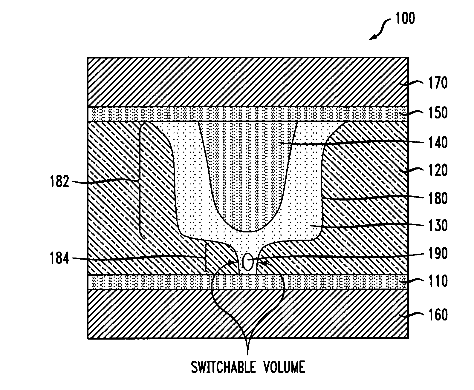
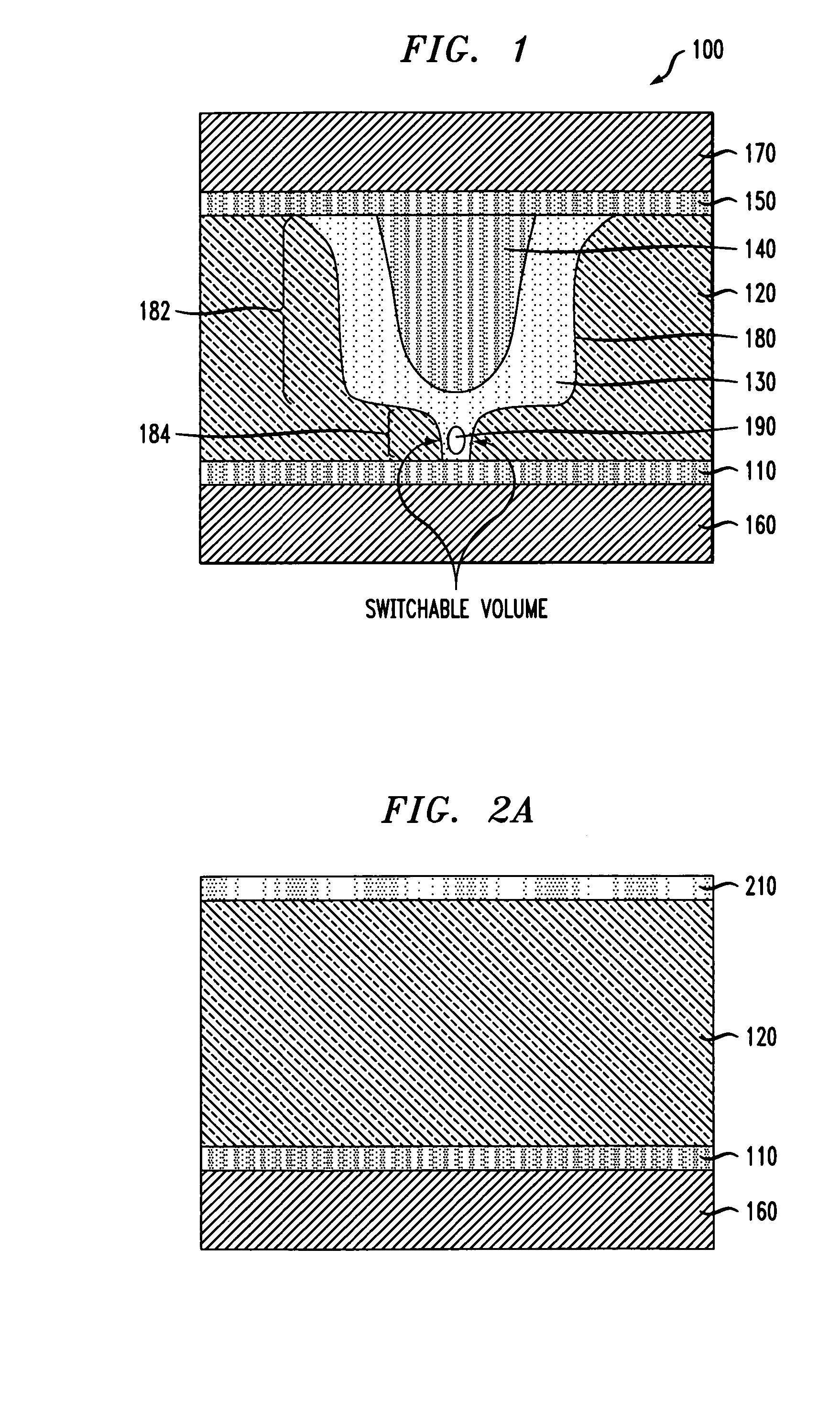
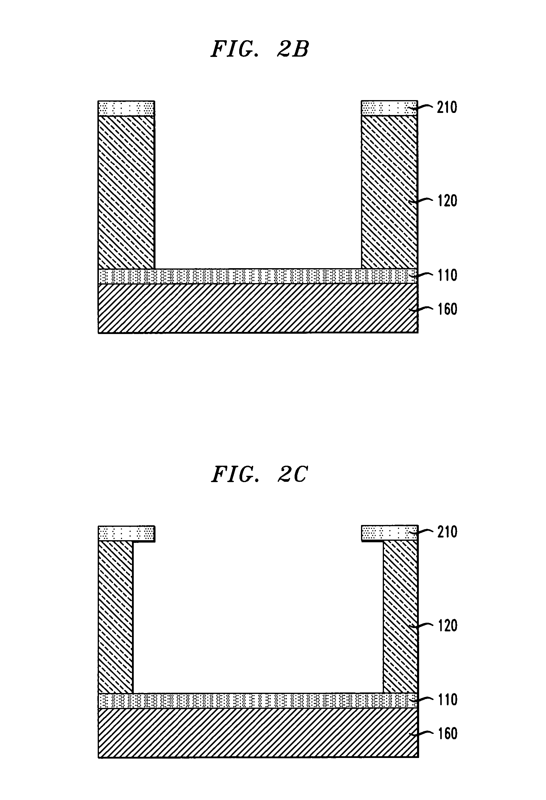
[0012]This invention will be illustrated herein in conjunction with exemplary memory cells for use in integrated circuits and methods for forming such memory cells. It should be understood, however, that the invention is not limited to the particular materials, features and processing steps shown and described herein. Modifications to the illustrative embodiments will become apparent to those skilled in the art.

[0013]Particularly with respect to processing steps, it is emphasized that the descriptions provided herein are not intended to encompass all of the processing steps which may be required to successfully form a functional integrated circuit device. Rather, certain processing steps which are conventionally used in forming integrated circuit devices, such as, for example, wet cleaning and annealing steps, are purposefully not described herein for economy of description. However one skilled in the art will readily recognize those processing steps omitted from these generalized d...


PUM


Abstract

A memory cell comprises a dielectric layer and a phase change material. The dielectric layer defines a trench having both a wide portion and a narrow portion. The narrow portion is substantially narrower than the wide portion. The phase change material, in turn, at least partially fills the wide and narrow portions of the trench. What is more, the phase change material within the narrow portion of the trench defines a void. Data can be stored in the memory cell by heating the phase change material by applying a pulse of switching current to the memory cell. Advantageously, embodiments of the invention provide high switching current density and heating efficiency so that the magnitude of the switching current pulse can be reduced.

Description

FIELD OF THE INVENTION[0001]This invention relates to memory cells in integrated circuits, and, more particularly, to memory cells comprising phase-change materials.BACKGROUND OF THE INVENTION[0002]The possibility of using phase change materials (PCMs) in nonvolatile memory cells has recently gained momentum as more is learned about these materials and their integration into integrated circuits. When incorporated in a memory cell, these materials can be toggled between higher and lower electrical resistance states by applying a pulse of electrical current (“switching current pulse”) to the memory cell. Subsequently, after writing to a memory cell in this way, the electrical resistance state of the given memory cell can be determined (i.e., read) by applying a low magnitude sensing voltage to the material in order to determine its electrical resistance state.[0003]Currently, binary and ternary chalcogenide alloys such as doped SbTe and Ge2Sb2Te5 (GST) are showing the greatest promise...

Claims


Application Information

Patent Timeline
Patent Type & Authority Patents(United States)
IPC IPC(8): H01L47/00
CPCH01L45/06H01L45/1233H01L45/1246H01L45/144H01L45/1625H01L45/1666H10N70/828H10N70/231H10N70/026H10N70/061H10N70/8828H10N70/826
Inventor BREITWISCH, MATTHEW J.LAM, CHUNG HONPHILIPP, JAN BORISROSSNAGEL, STEPHEN M.SCHROTT, ALEJANDRO GABRIEL
Owner INFINEON TECHNOLOGIES NORTH AMERICA CORPORATION
Why Eureka
Try Eureka