Method for making an electronic device including a poled superlattice having a net electrical dipole moment

a superlattice and net electrical dipole moment technology, applied in piezoelectric/electrostrictive devices, device materials, piezoelectric/electrostrictive/magnetostrictive devices, etc., can solve the problem of polarization hysteresis characteristic degrading with increasing cycles, pzt ceramics have fallen out of favor in many commercial applications and materials, and drawbacks associated

Active Publication Date: 2009-04-14
ATOMERA INC
View PDF63 Cites 95 Cited by
  • Summary
  • Abstract
  • Description
  • Claims
  • Application Information

AI Technical Summary

Problems solved by technology

However, PZT ceramics have fallen out of favor in many commercial applications and materials due to concerns over its toxicity (i.e., because they include lead).
Accordingly, there is a need for piezoelectric and pyroelectric materials than can provide desired properties such as those discussed above, yet do not have the drawbacks associated with traditional materials such as toxicity, for example.
One problem with reading from a Ferroelectric Random Access Memory (FeRAM) is that the polarization hysteresis characteristic degrades with increasing cycles of the reading process.
While the latter provides somewhat better anti-fatigue properties, these alloys require relatively complicated fabrication processes.
Since the conventional Si micromachining technology coupled with silicon oxide or nitride and metal is limited in its ability to produce fine-scale capacitors, utilization of ferroelectrics with polarization hysteresis has gained attention in non-volatile memory technology development.

Method used


Image

  • Method for making an electronic device including a poled superlattice having a net electrical dipole moment
  • Method for making an electronic device including a poled superlattice having a net electrical dipole moment
  • Method for making an electronic device including a poled superlattice having a net electrical dipole moment

Examples


Embodiment Construction

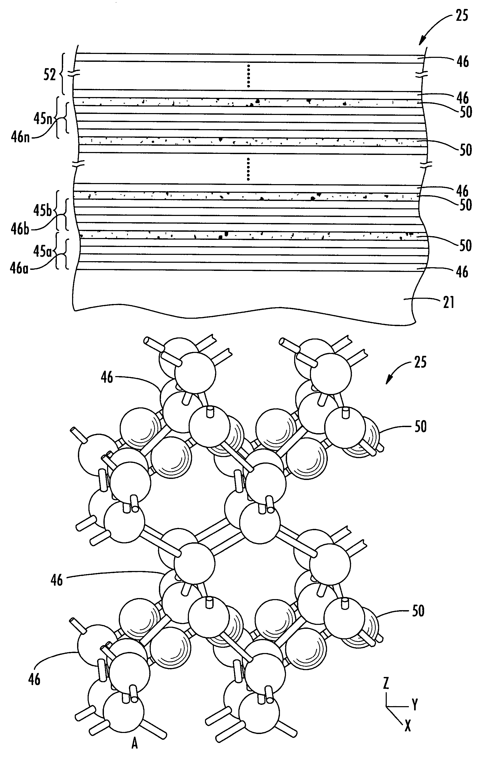
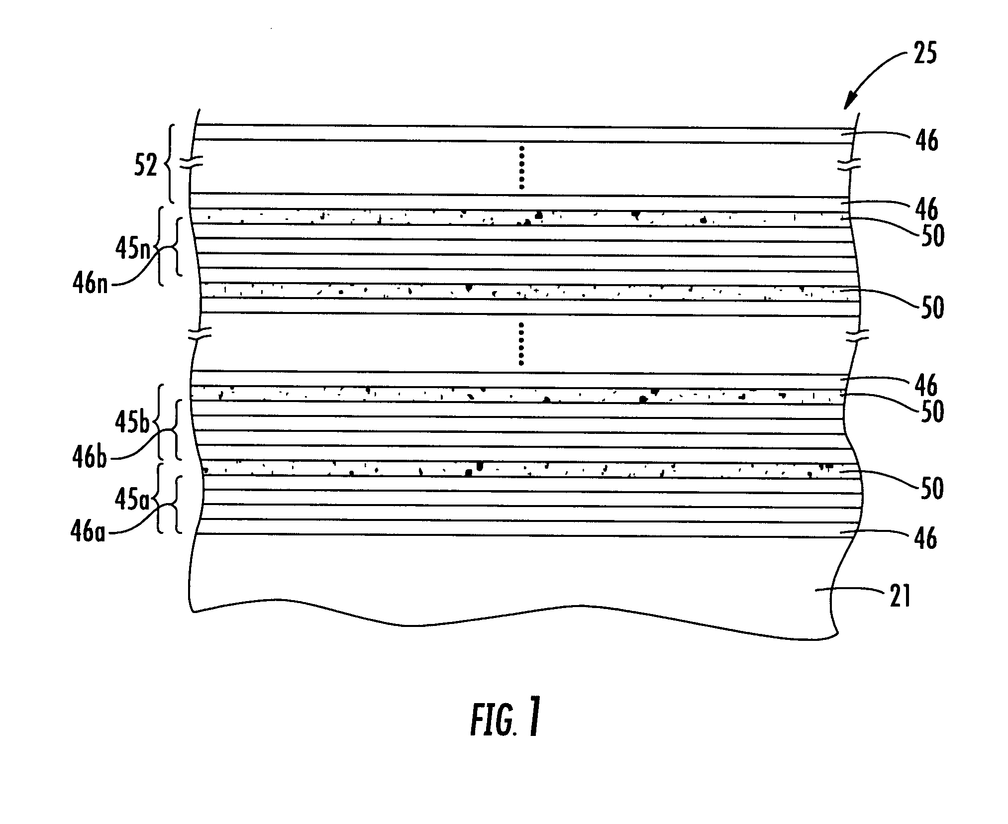
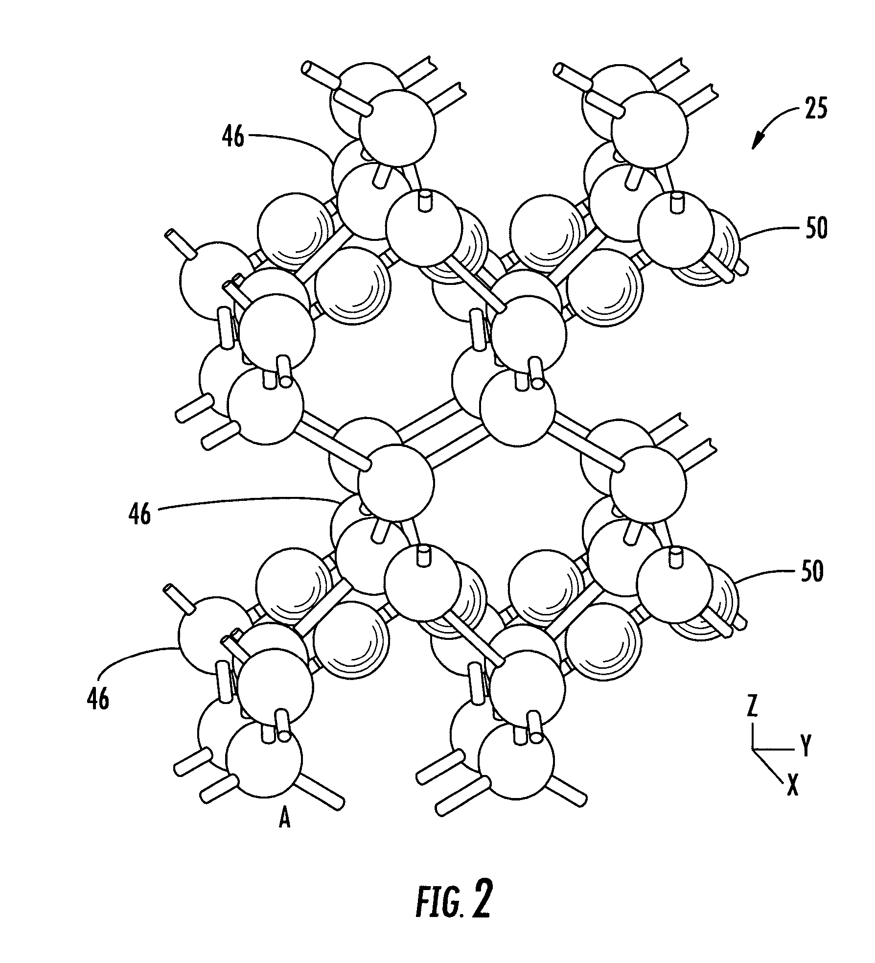
[0062]The present invention will now be described more fully hereinafter with reference to the accompanying drawings, in which preferred embodiments of the invention are shown. This invention may, however, be embodied in many different forms and should not be construed as limited to the embodiments set forth herein. Rather, these embodiments are provided so that this disclosure will be thorough and complete, and will fully convey the scope of the invention to those skilled in the art. Like numbers refer to like elements throughout, and prime notation is used to indicate similar elements in different embodiments.

[0063]The present invention relates to controlling the properties of semiconductor materials at the atomic or molecular level. Further, the invention relates to the identification, creation, and use of improved materials for use in semiconductor devices.

[0064]Applicants theorize, without wishing to be bound thereto, that certain superlattices as described herein reduce the ef...


PUM


Abstract

A method for making an electronic device may include forming a poled superlattice comprising a plurality of stacked groups of layers and having a net electrical dipole moment. Each group of layers of the poled superlattice may include a plurality of stacked semiconductor monolayers defining a base semiconductor portion and at least one non-semiconductor monolayer thereon. The at least one non-semiconductor monolayer may be constrained within a crystal lattice of adjacent base semiconductor portions, and at least some semiconductor atoms from opposing base semiconductor portions may be chemically bound together through the at least one non-semiconductor monolayer therebetween. The method may further include coupling at least one electrode to the poled superlattice.

Description

CROSS-REFERENCE TO RELATED APPLICATIONS[0001]The present applications claims the benefit of U.S. Provisional Application Nos. 60 / 753,141, 60 / 753,143, 60 / 752,990, 60 / 753,120, 60 / 753,142, 60 / 752,985, and 60 / 752,984, all filed Dec. 22, 2005, all of which are hereby incorporated herein in their entireties by reference.FIELD OF THE INVENTION[0002]The present invention relates to the field of semiconductors, and, more particularly, to semiconductor devices comprising superlattices and associated methods.BACKGROUND OF THE INVENTION[0003]Piezoelectric materials are used in numerous devices where a conversion of mechanical energy into electrical energy or vice-versa is required. More particularly, in piezoelectric materials induced charges are proportional to mechanical stress. Piezoelectric materials also conversely have a geometric strain that is proportional to an applied electric field. This phenomenon is based upon the dependence of the polarization (i.e., surface charge) of the materia...

Claims


Application Information

Patent Timeline
Patent Type & Authority Patents(United States)
IPC IPC(8): H01L21/00
CPCB82Y10/00H01L21/28291H01L29/151H01L29/78391H01L41/18H01L41/314H01L29/40111H10N30/852H10N30/074
Inventor HALILOV, SAMEDHUANG, XIANGYANGDUKOVSKI, ILIJAYIPTONG, JEAN AUGUSTIN CHAN SOW FOOKMEARS, ROBERT J.HYTHA, MAREKSTEPHENSON, ROBERT JOHN
Owner ATOMERA INC
Why Eureka
Try Eureka