High yield, high density on-chip capacitor design

a capacitor design and high density technology, applied in the field of capacitors, can solve the problems of reduced semiconductor chip area availability for other circuit structures, large chip area footprints of moscap capacitors in integrated circuits, and high production costs

Inactive Publication Date: 2009-04-14
GLOBALFOUNDRIES INC
View PDF8 Cites 18 Cited by
  • Summary
  • Abstract
  • Description
  • Claims
  • Application Information

AI Technical Summary

Benefits of technology

[0019]Aspects of the present invention address these matters, and others.

Problems solved by technology

However, the reactance resistance of the bypass capacitor is generally required to be as low as possible for a target AC noise signal frequency.
However, MOSCAP capacitors require large chip area footprints in integrated circuits (IC).
Accordingly, prior art design requirements typically result in requiring large semiconductor chip footprint areas or real estate for a bypass capacitor structure, resulting in high production costs and reduced semiconductor chip area availability for other circuit structures.
Moreover, current leakage during a semiconductor circuit's idle mode is known to result in increased power consumption.

Method used


Image

  • High yield, high density on-chip capacitor design
  • High yield, high density on-chip capacitor design
  • High yield, high density on-chip capacitor design

Examples


Embodiment Construction

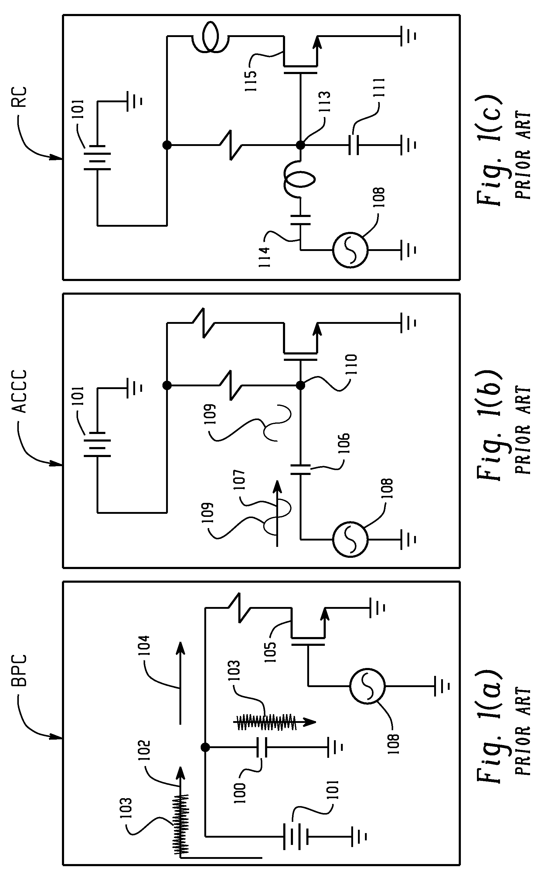
[0036]FIG. 2 illustrates a prior art by-pass capacitor structure 200, wherein a MOSCAP 210 is configured to bypass AC noise signals 203 from a noisy power signal 202 from a power supply 201 prior to supply of power to a circuit structure 205. The bypass MOSCAP 210 flows AC noise signals 203 into ground G, thus providing a clean DC power signal 204 to the circuit 205. Some of the noisy power signal 202 current is also lost as leakage 206 by the MOSCAP 210.

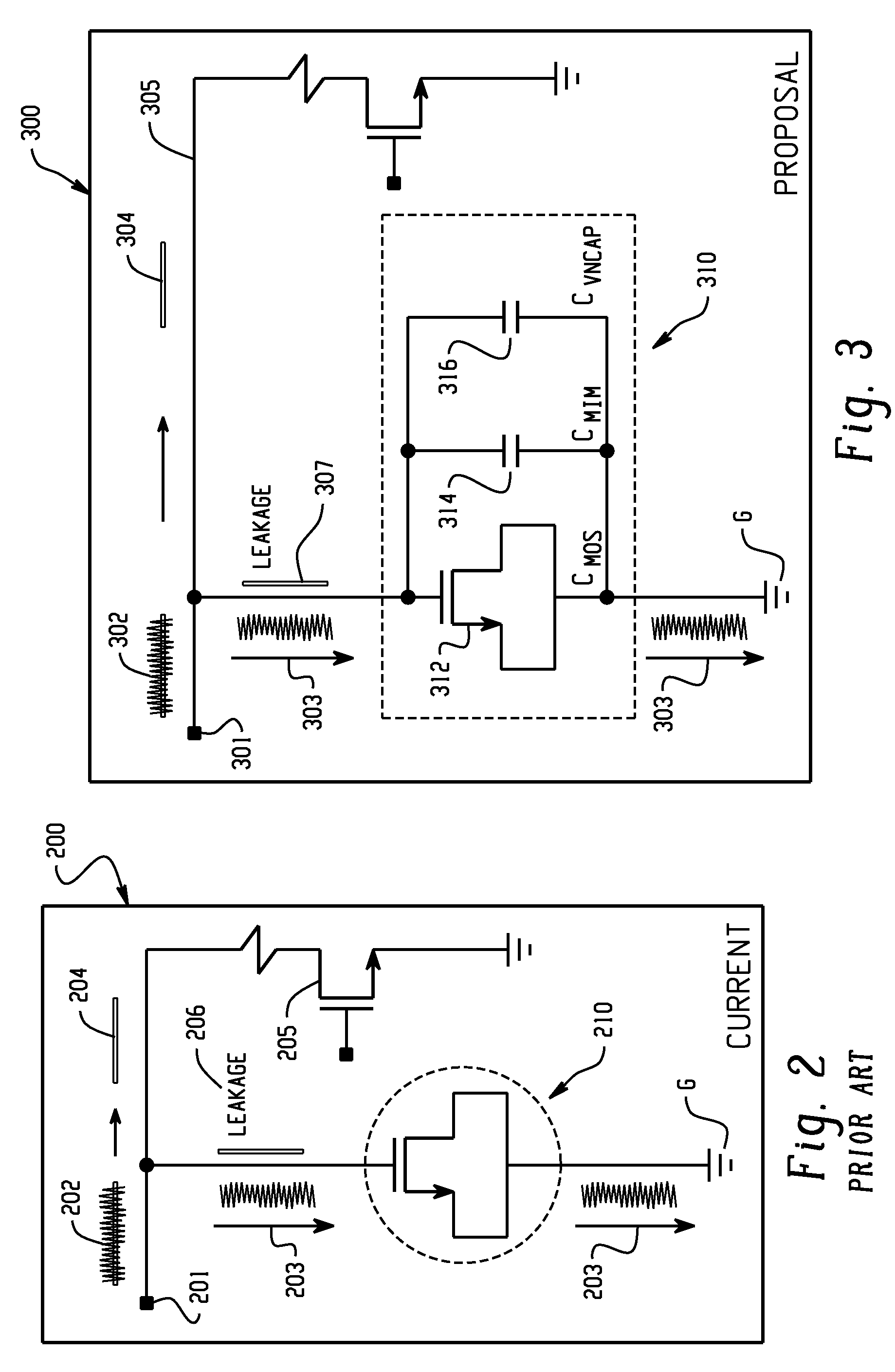
[0037]FIG. 3 illustrates a by-pass capacitor structure 300 according to the present invention with a multicapacitor circuit element 310, the multicapacitor element 310 comprising three capacitors 312, 314 and 316 arranged in parallel between a noisy power signal 302 and ground G. The multicapacitor element 310 bypasses AC noise signals 303 from the noisy power signal 302 from the power supply 301 into ground G prior to supply of power to a circuit structure 305, thus providing a clean DC power signal 304 to the circuit 305. Some of ...


PUM


Abstract

A capacitance circuit assembly mounted on a semiconductor chip, and methods for forming the same, are provided. A plurality of divergent capacitors is provided in a parallel circuit connection between first and second ports, the plurality providing at least one Metal Oxide Silicon Capacitor and at least one Vertical Native Capacitor or Metal-Insulator-Metal Capacitor. An assembly has a vertical orientation, a Metal Oxide Silicon capacitor located at the bottom and defining a footprint, with a middle Vertical Native Capacitor having a plurality of horizontal metal layers, including a plurality of parallel positive plates alternating with a plurality of parallel negative plates. In another aspect, vertically asymmetric orientations provide a reduced total parasitic capacitance.

Description

FIELD OF THE INVENTION[0001]This invention relates to capacitors on semiconductor chips. More particularly, the invention relates to silicon semiconductor chip capacitor structures comprising multiple parallel divergent capacitors.BACKGROUND OF THE INVENTION[0002]To enhance the understanding of the discussion that follows, the abbreviations and terms listed below will have the definitions as shown, the meaning and significance of which will be readily apparent to one skilled in the art of circuit board capacitor structures:[0003]ADC—Analog to digital converter;[0004]BEOL—Back end of line;[0005]CA—Tungsten contact between metal and polysilicon;[0006]Csub—Adjustable capacitor;[0007]DAC—Digital to analog converter;[0008]FEOL—Front end of line;[0009]MIMCAP—Metal-insulator-metal capacitor;[0010]MOS—Metal oxide silicon;[0011]RF—Radio frequency;[0012]VNCAP—Vertical native capacitor.[0013]On-chip capacitors are critical components of integrated circuits that are fabricated on silicon semico...

Claims


Application Information

Patent Timeline
Patent Type & Authority Patents(United States)
IPC IPC(8): H01G4/38H01G4/00H01L21/20H01L27/108H01L29/94
CPCH01L23/5223H01L27/0688H01L27/0805H01L27/0811H01L2924/3011H01L2924/0002H01L2924/00H01L27/06
Inventor KIM, JONGHAEKIM, MOON J.PLOUCHART, JEAN-OLIVIERTRZCINSKI, ROBERT E.
Owner GLOBALFOUNDRIES INC
Why Eureka
Try Eureka