Shielding arrangement for electronic device

Inactive Publication Date: 2009-04-14
BI LINK
View PDF78 Cites 29 Cited by
  • Summary
  • Abstract
  • Description
  • Claims
  • Application Information

AI Technical Summary

Benefits of technology

[0032]The various aspects and embodiments of the invention demonstrate the advantages of providing a cover portion and sidewall of an electronic device that includes a conductive inside surface to provide shielding for an electronic component. According to one aspect, a separate shielding element mounted beneath a device cover plate can be eliminated. A significant vertical space and lateral space can be saved to a

Problems solved by technology

It is well known that electronic signals within electronic packages emit electromagnetic energy from the package, which causes electromagnetic interference (EMI) in other electric signals.
On the other hand, electrostatic discharge (ESD) is also another import

Method used


Image

  • Shielding arrangement for electronic device
  • Shielding arrangement for electronic device
  • Shielding arrangement for electronic device

Examples


Example

[0049]While this invention is susceptible of embodiment in many different forms, there are shown in the drawings, and will be described herein in detail, specific embodiments thereof with the understanding that the present disclosure is to be considered as an exemplification of the principles of the invention and is not intended to limit the invention to the specific embodiments illustrated.

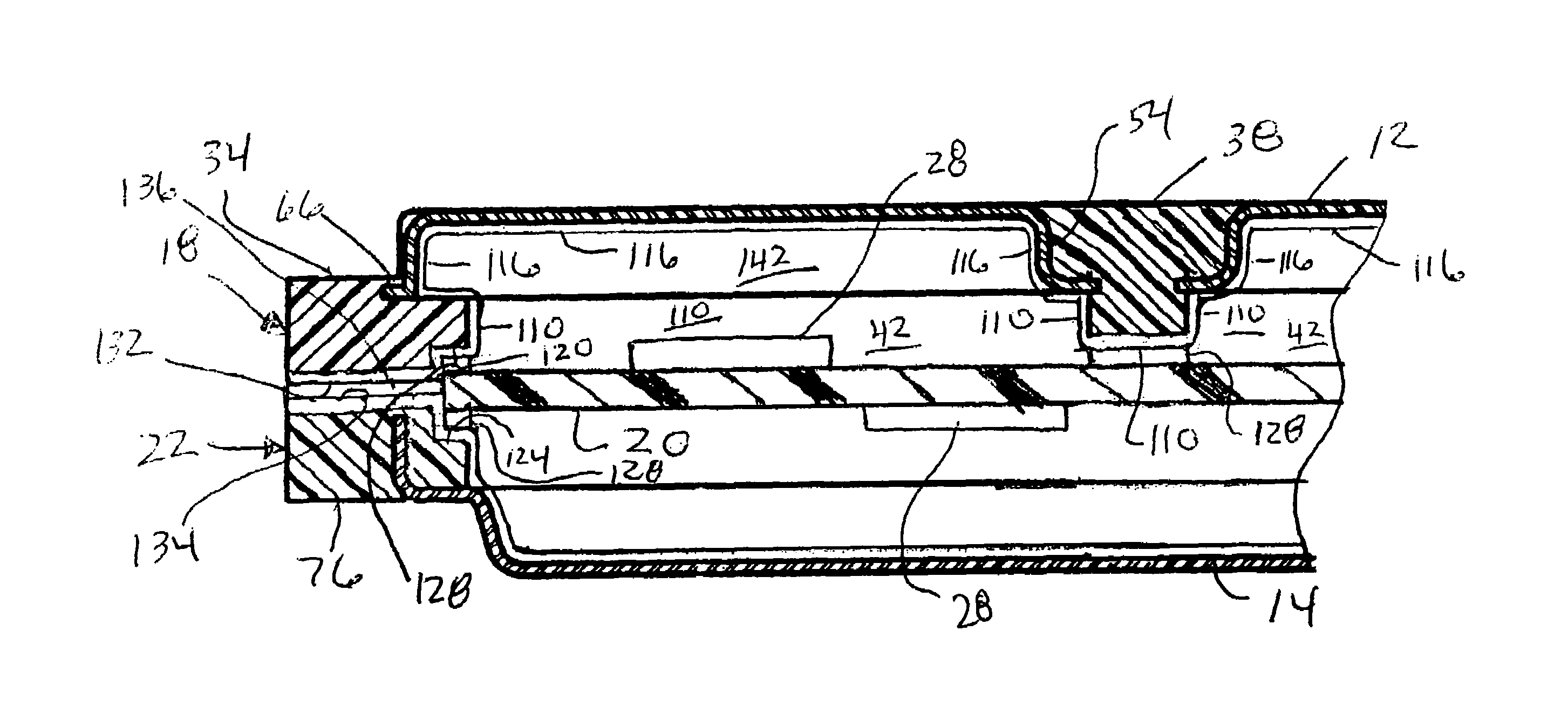
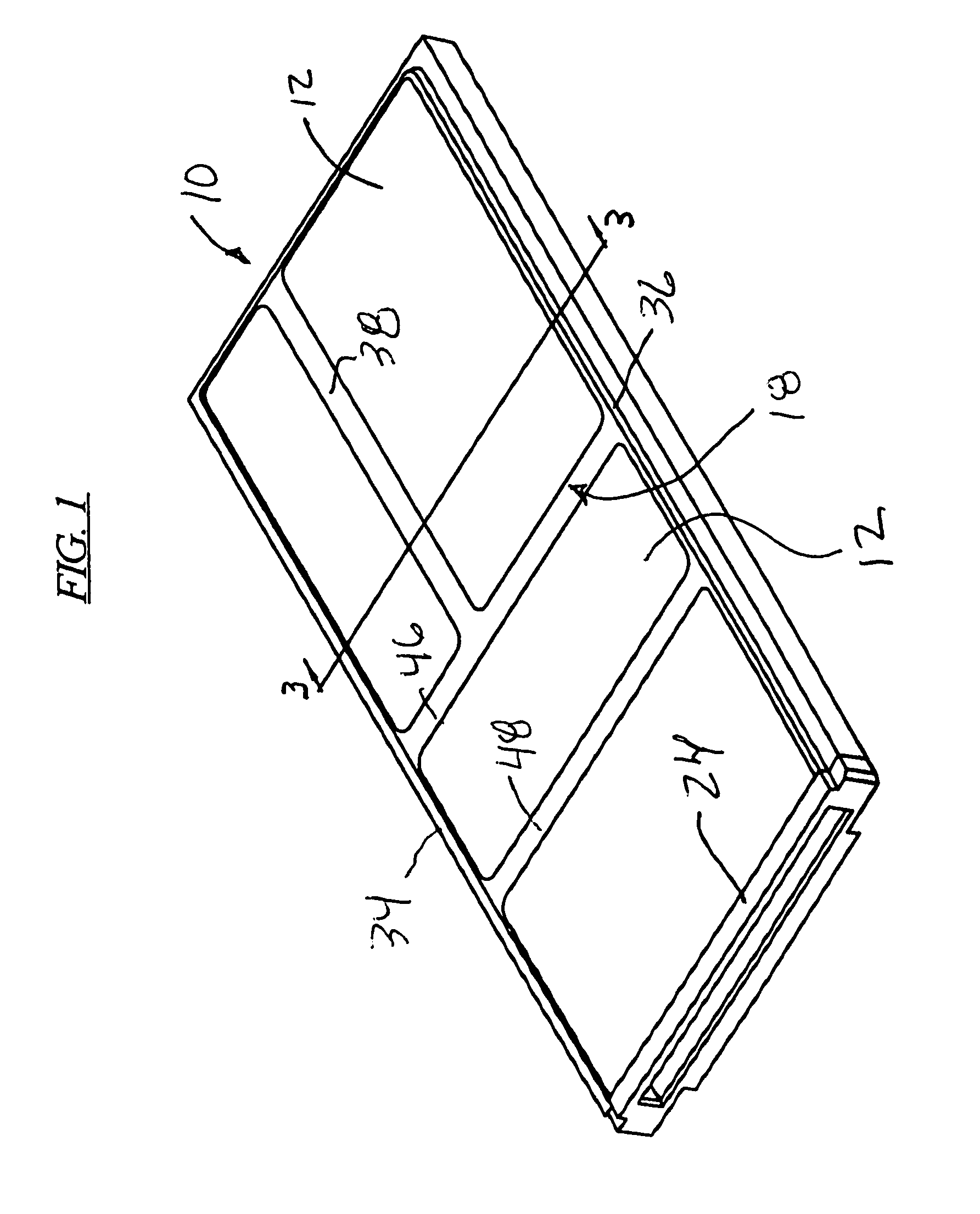
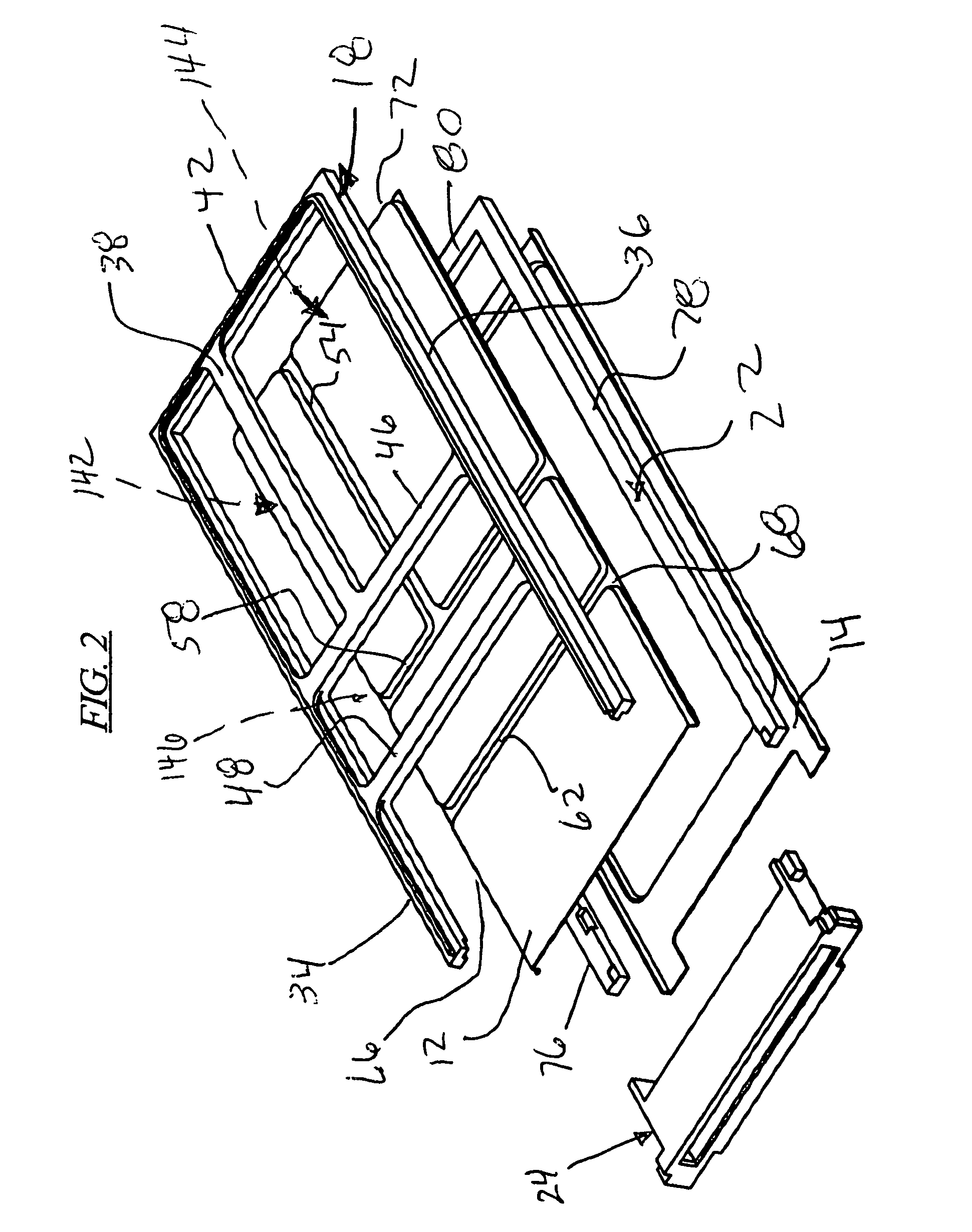
[0050]FIG. 1 illustrates an electronic device 10, in the form of a peripheral card, for providing an outside device (not shown), such as a computer system, with a plug-in signal processing module or memory module. The device 10 includes first and second cover portions, such as in the form of metallic top and bottom covers 12, 14, an upper frame 18, a circuit board 20 (shown in FIG. 3), a lower frame 22, and an end connector 24. The upper and lower frames 18, 22 are preferably molded plastic or polymer parts. The end connector 24 is adapted to electrically mate with a corresponding connector (not ...


PUM


Abstract

A shielding arrangement for an electronic component mounted on a circuit board includes a shield formed by a frame sidewall arranged to be oriented upstanding from the circuit board and surrounding the electronic component mounted on the circuit board. A first cover portion substantially closes the surrounding sidewall, enclosing the electronic component on the circuit board. A conductive layer, formed by vacuum deposition covers an inside surface of the surrounding sidewall and an inside surface of the first cover portion, continuously. As an alternative to the conductive layer, the frame can be composed of an electrically conductive plastic. The first cover portion can be a stamped metal plate integrated with the frame by overmolding.

Description

[0001]This application claims the benefit of U.S. Provisional Application 60 / 771,247 filed Feb. 8, 2006.TECHNICAL FIELD OF THE INVENTION[0002]The present invention relates generally to shielding of electronic components and particularly to shielding of memory media and I / O device containers, and more particularly to shielding of a casing for printed circuit boards that conforms to standards set by PCMCIA, JEDIC, ISO, etc. for peripheral devices.BACKGROUND OF THE INVENTION[0003]As computing devices are reduced in size, there is reduced available space for storage devices such as a hard disk drive or an I / O device. In order to expand a portable, laptop, or any other type of computer's capacity and functioning capability, manufacturers have devised “plug-in” peripheral cards in the form of printed circuit boards contained within an exterior casing. The Personal Computer Memory Card International Association (PCMCIA) and comparable organizations have established certain size and shape s...

Claims


Application Information

Patent Timeline
IPC IPC(8): H05K1/14
CPCH05K9/0084
Inventor ZIBERNA, FRANK J.
Owner BI LINK
Why Eureka
Try Eureka