
Chip card with simultaneous contact and contact-less operations

a chip card and contactless technology, applied in the field of chip cards, can solve the problems of inductive coupling to the antenna coil, easy wear of the contact bank 104/b>, and insufficient power supply to the ic chip , achieve the effect of more stable contact bias voltag

Active Publication Date: 2009-04-21
SAMSUNG ELECTRONICS CO LTD
View PDF2 Cites 7 Cited by
  • Summary
  • Abstract
  • Description
  • Claims
  • Application Information

AI Technical Summary

Benefits of technology

The present invention is a chip card that can process both contact data and contact-less data simultaneously. This allows for multiple functions to be performed by the chip card, such as making a phone call and making a payment, simultaneously. The chip card includes a micro-computer and interfaces for receiving and processing the data. The micro-computer can also select between the contact bias voltage and the contact-less bias voltage based on the availability of each. Overall, the chip card provides enhanced functionality and flexibility for various applications.

Problems solved by technology

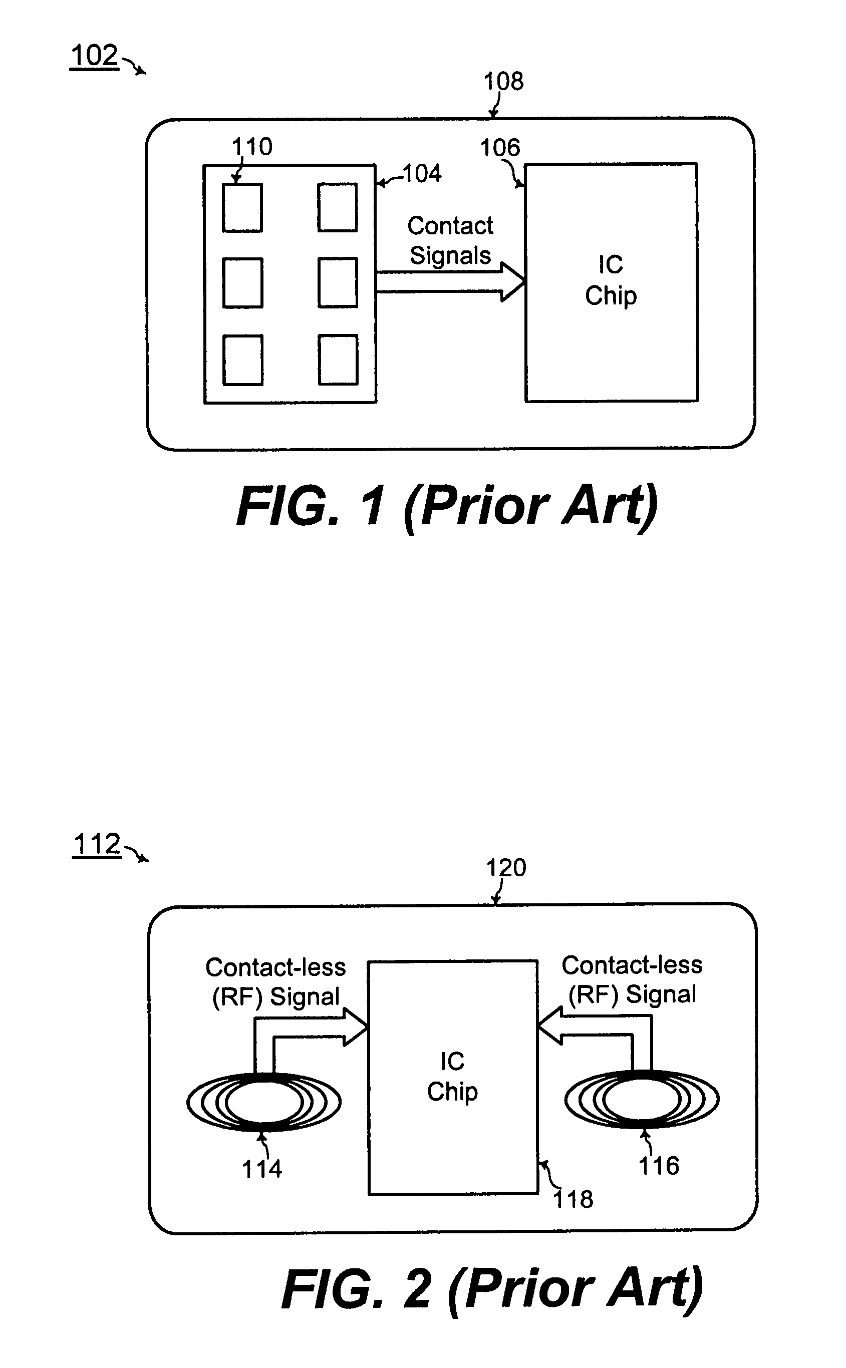
A disadvantage of the chip card 102 of the contact type in FIG. 1 is that the contacts of the contact bank 104 are easily worn due to careless treatment or to frequent contact with a terminal.
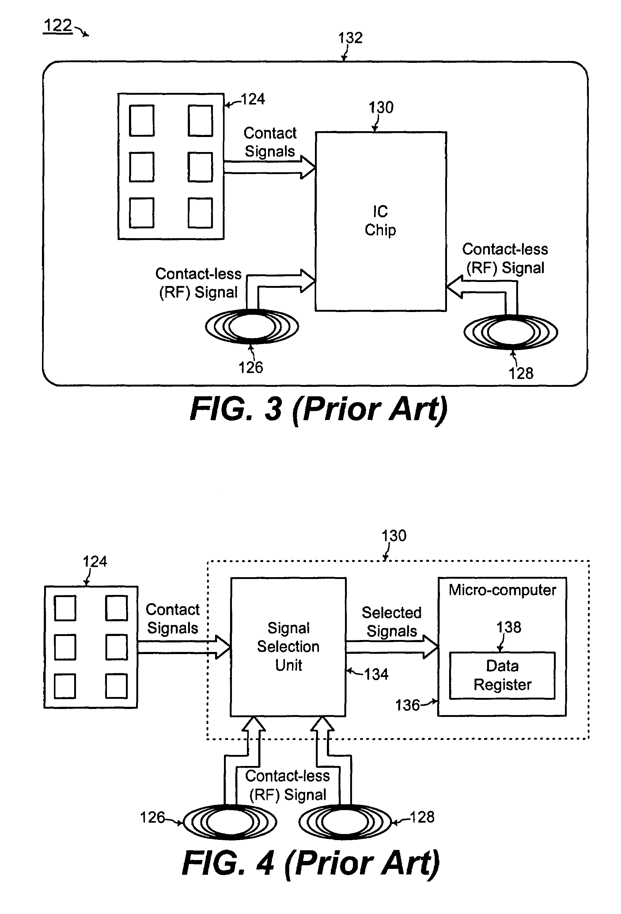
A disadvantage of the chip card 112 of the contact-less type in FIG. 2 is that supply power provided to the IC chip 118 via inductive coupling to the antenna coils 114 and 116 is unstable due to noise between the chip card 120 and a contact-less based terminal.
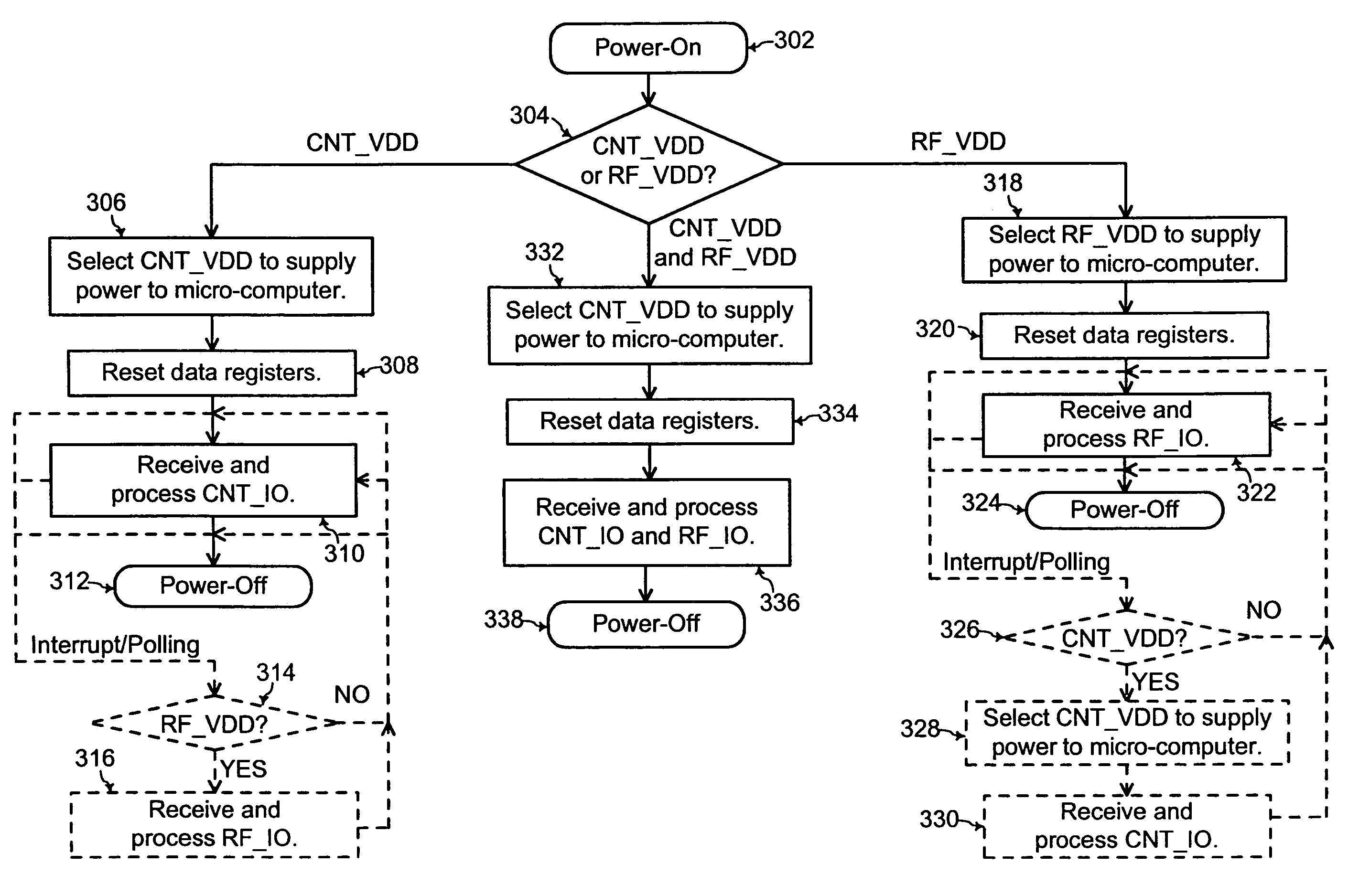
In either FIG. 5 or FIG. 6 of the prior art, processing of CNT_IO (contact data) or RF_IO (contact-less data) may be prematurely aborted, and the results of such processing are disadvantageously lost.

Method used


Image

  • Chip card with simultaneous contact and contact-less operations
  • Chip card with simultaneous contact and contact-less operations
  • Chip card with simultaneous contact and contact-less operations

Examples


Embodiment Construction

[0041]Referring to an embodiment of the present invention in FIG. 7, a chip card 200 of the combined type includes both a contact bank 202 having a plurality of contacts 204 and at least one antenna coil (a first antenna coil 206 and a second antenna coil 208 in the example of FIG. 7). The contact bank 202 and the first and second antenna coils 206 and 208 are coupled to an IC (integrated circuit) chip 210 (outlined in dashed lines in FIG. 7).

[0042]The contact bank 202, the antenna coils 206 and 208, and the IC chip 210 are formed onto a substrate (not shown in FIG. 7) for the chip card 200. The substrate for the chip card 200 typically has a shape similar to a credit-card, and physical placement of the contact bank 202, the antenna coils 206 and 208, and the IC chip 210 onto the substrate is dictated by ISO standards as known to one of ordinary skill in the art.

[0043]The IC chip 210 includes a micro-computer 212 (outlined in dashed lines in FIG. 7) and a contact interface 214 coupl...


PUM


Abstract

A chip card receives and processes what-ever combination of contact data and contact-less data is available to allow multiple functionalities for the chip card. A micro-computer of the chip card is adapted to simultaneously receive and process contact data from a contact interface and contact-less data from a contact-less interface. In addition, the chip card includes a power voltage selector for selecting a contact bias to supply power to the micro-computer when-ever the contact bias voltage is available since the contact bias voltage is more stable than a contact-less bias voltage.

Description

CROSS-REFERENCE TO RELATED APPLICATION(S)[0001]The present application is a continuation of an earlier filed copending patent application with Ser. No. 10 / 852,610 filed on May 24, 2004, now U.S. Pat. No. 7,246,750 for which priority is claimed. This earlier filed copending patent application with Ser. No. 10 / 852,610 is in its entirety incorporated herewith by reference.[0002]The present application also claims priority under 35 USC § 119 to Korean Patent Application No. 2003-0062251, filed on Sep. 5, 2003, in the Korean Intellectual Property Office, the disclosure of which is incorporated herein in its entirety by reference. A certified copy of Korean Patent Application No. 2003-0062251 is contained in the parent copending patent application with Ser. No. 10 / 852,610.TECHNICAL FIELD[0003]The present invention relates generally to chip cards (i.e., “smart cards”), and more particularly, to a chip card having a contact interface, a contact-less interface, and a micro-computer adapted f...

Claims


Application Information

Patent Timeline
Patent Type & Authority Patents(United States)
IPC IPC(8): G06K19/00B42D25/305G06K19/07G06K19/077
CPCG06K19/07G06K19/07769
Inventor CHO, ZANG-HEE
Owner SAMSUNG ELECTRONICS CO LTD
Learn More