Method for manufacturing semiconductor device

a semiconductor and manufacturing technology, applied in the field of semiconductor devices, can solve problems such as deterioration of tft characteristics, and achieve the effect of reliable semiconductor apparatus

Inactive Publication Date: 2009-04-21
SEMICON ENERGY LAB CO LTD
View PDF19 Cites 22 Cited by
  • Summary
  • Abstract
  • Description
  • Claims
  • Application Information

AI Technical Summary

Benefits of technology

[0014]It is an object of the present invention to prevent the etching damage during dry etching of the interlayer insulating film after forming the TFT in the processes of manufacturing a TFT. Further, it is another object of the present invention to provide a method for not deteriorating the transistor characteristic especially in the TFT having a minute structure.
[0016]According to the present invention, when an electrode or a wiring electrically connected to the TFT which is formed beneath an insulating film in which the contact hole is formed, a conductive material film which does not have electrical contact with the TFT is formed over the electrode or wiring. Accordingly, damage during etching can be prevented at the time of performing etching for forming the contact hole.
[0017]By forming such a conductive material film, the charged particles generated by plasma can be prevented from dispersing into the conductive material film to reach the TFT in the lower layer. Therefore, it is possible to suppress the deterioration in the transistor characteristic of the TFT.
[0018]In other words, the charged particles generated by plasma are trapped in the conductive material film having floating potential and does not reach the TFT. Therefore, the deterioration of the TFT characteristic, for example generation of the damage to the gate insulating film of the TFT due to the injection of the charged particles, can be prevented.
[0020]The present invention includes the following structure. Hereinafter, a method for minimizing the damage at the time of forming the contact hole in the insulating film formed over the electrode or wiring after forming the electrode or wiring connected to the TFT is described. This is because a large-sized electrode in the upper part formed of the electrode or wiring functions as an antenna, which gathers the charged particles, in etching to form the contact hole after forming the large-sized electrode in the upper part connected to the TFT through the electrode or wiring. Therefore, it is apparent to suppress the etching damage and thus the advantageous effect of the present invention is prominent. Of course, an insulating film in any layer can be etched as long as etching is performed to form the contact hole.
[0039]According to the present invention, although dry etching is performed to the interlayer insulating film after forming the electrode, the charged particles generated by plasma during dry etching are not injected into the TFT through an insulating film. Therefore, the transistor characteristic of the TFT is not deteriorated; thus, a reliable semiconductor apparatus can be obtained.

Problems solved by technology

The damage during dry etching after forming the electrode is considered to result from an insulating material, such as an interlayer insulating film or a resist, only which exists over an electrode or a wiring electrically connected to the TFT at the time of forming a contact hole in the interlayer insulating film after forming the TFT.
This is considered to result in deteriorating the TFT characteristic.

Method used


Image

  • Method for manufacturing semiconductor device
  • Method for manufacturing semiconductor device
  • Method for manufacturing semiconductor device

Examples


embodiment 1

[0110]In this embodiment, a TFT in which a contact hole is formed with a metal cap film and a TFT in which a contact hole is formed without a metal cap film are compared in terms of the transistor characteristic with reference to FIGS. 4A and 4B, FIGS. 5 to 8, and FIGS. 29A and 29B.

[0111]FIG. 29A shows the characteristic of gate voltage and drain current of the n-channel TFT manufactured without forming a metal cap film. FIG. 4A shows the characteristic of gate voltage and drain current of the n-channel TFT manufactured by forming a metal cap film.

[0112]In each FIG. 4A and FIG. 29A, a horizontal axis indicates gate voltage (VG [V]), and a vertical axis indicates drain current (ID [A]).

[0113]In FIG. 4A and FIG. 29A, the channel length (L) and the channel width (W) of the n-channel TFT are each 3 μm and 2 μm, and the thickness of a gate insulating film (referred to as “Tox” in this specification) is 55 nm.

[0114]In each FIG. 4A and FIG. 29A, a solid line indicates the TFT characteristi...

embodiment 2

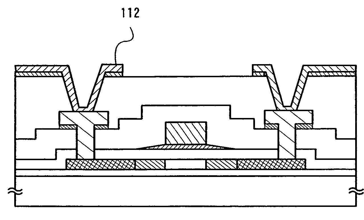
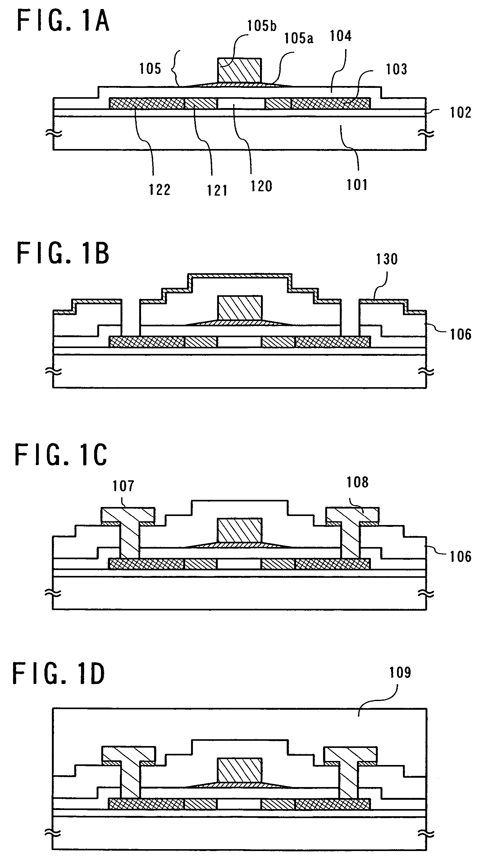
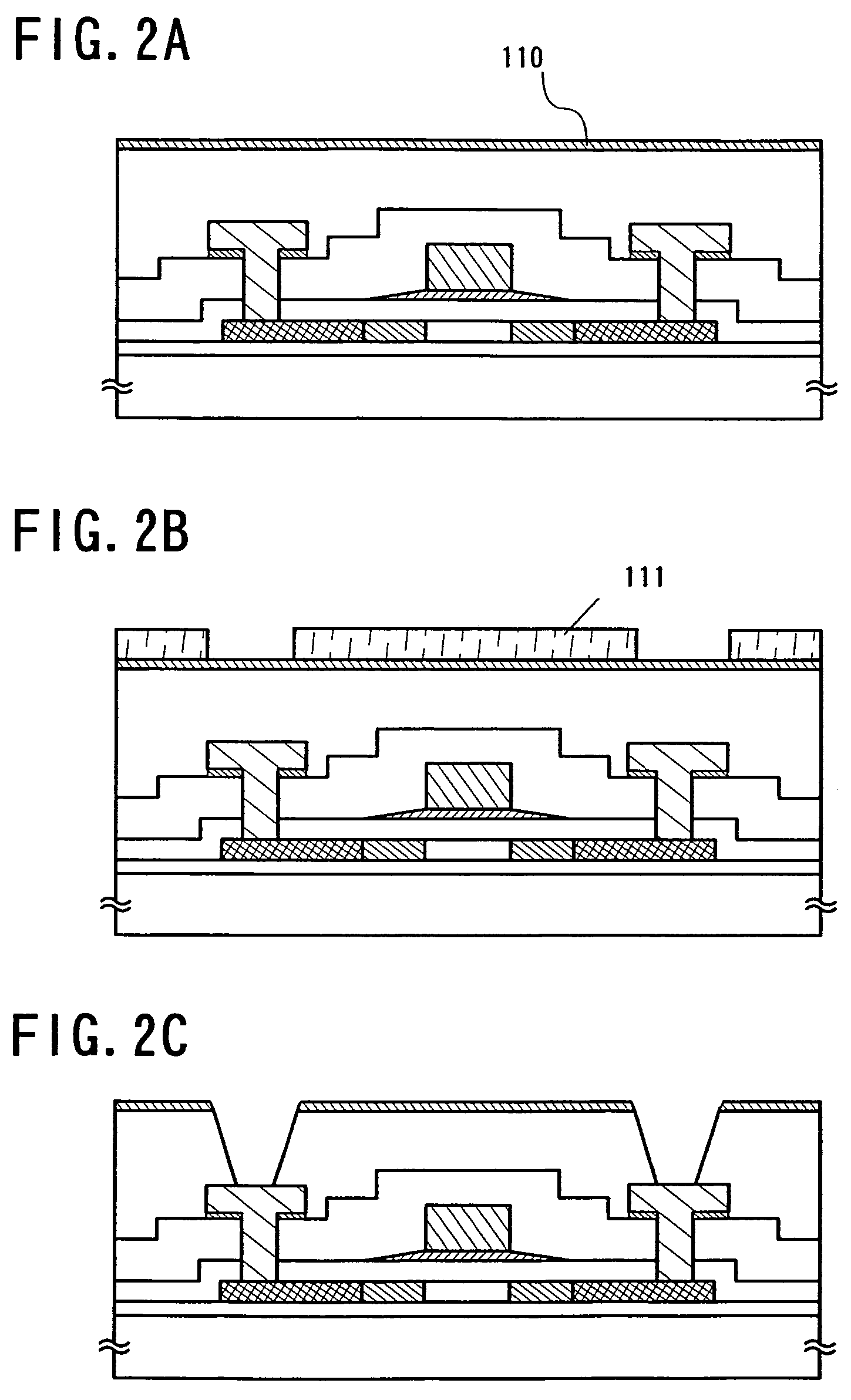
[0144]This embodiment describes a method for manufacturing an active matrix liquid crystal display device in which a reverse staggered TFT is used as a switching element. Further, FIGS. 9A to 9E each illustrate a cross section of a manufacturing process, and FIG. 10 illustrates a top view.

[0145]Firstly, a base insulating film 611 is formed over a substrate 610. An insulating film such as a silicon oxide film, a silicon nitride film, or silicon oxide film containing nitrogen (SiOxNy) is preferably used as the base insulating film 611. A heat-resistant plastic substrate that can withstand a processing temperature of the manufacturing process can be used besides a non-alkaline glass substrate as the substrate 610. In the case of a reflective liquid crystal display device, a semiconductor substrate such as single crystal silicon, a metal substrate such as stainless, or a ceramic substrate in which an insulating layer is provided on the surface may be applied to the substrate.

[0146]Then,...

embodiment 3

[0174]This embodiment describes an example of using a droplet discharging method for dropping liquid crystals. In this embodiment, FIGS. 1A to 11D, FIGS. 12A to 12D, FIGS. 13A and 13B, FIGS. 14A and 14B, and FIG. 15 each illustrate an example of manufacturing a panel for taking four panels from one large-sized substrate 1110.

[0175]FIG. 11A illustrates a cross-sectional view in forming a liquid crystal layer by a dispenser (or ink jetting) method. A liquid crystal material 1114 is discharged, sprayed, or dropped from a nozzle 1118 of a droplet discharging device 1116 to cover a pixel portion 1111 surrounded by a sealant 1112. The droplet discharging device 1116 is moved in the direction indicated by an arrow in FIG. 11A. Further, an example of moving the nozzle 1118 is described; however, the nozzle may be secured and the substrate may be moved to form the liquid crystal layer.

[0176]FIG. 11B illustrates a perspective view. In FIG. 11B, the liquid crystal material 1114 is selectively ...


PUM


Abstract

The present invention provides a method for manufacturing a semiconductor device having high characteristic and reliability. The etching damage during dry etching after forming an electrode or a wiring over an insulating film is prevented. The damage is suppressed by forming a conductive layer so that charged particles due to plasma during dry etching are not generated in a semiconductor layer. Accordingly, it is an object of the invention to provide a method not for generating the deterioration of the transistor characteristic especially in a thin film transistor having a minute structure.

Description

BACKGROUND OF THE INVENTION[0001]1. Field of the Present Invention[0002]The present invention relates to a semiconductor apparatus comprising a circuit including a thin film transistor (hereinafter, referred to as a TFT) and a method for manufacturing the semiconductor apparatus. For example, the present invention relates to an electro-optical device typified by a liquid crystal display panel, an EL (an electroluminescence) display device, an EC display device, and the like. In addition, the present invention relates to an electric device for improving processing rate formed by using the TFT, for example a central processing unit (CPU), and a method for manufacturing the electric device. Further, the present invention relates to an electric apparatus equipped with these electro-optical device and electric device as the components.[0003]2. Description of the Related Art[0004]In recent years, a thin film transistor (TFT) is formed using a semiconductor film formed over a substrate hav...

Claims


Application Information

Patent Timeline
Patent Type & Authority Patents(United States)
IPC IPC(8): H01L21/302H01L21/461H01L21/77H01L21/84H01L31/20
CPCH01L27/1214H01L29/78621H01L27/1288
Inventor YAMAGUCHI, TETSUJIASANO, ETSUKOYAZAKI, NAOMIFUTAMURA, TOMOYANISHIKAWA, TOMOKO
Owner SEMICON ENERGY LAB CO LTD
Why Eureka
Try Eureka