Method of manufacturing a MOS transistor of a semiconductor device

a technology of metal oxide semiconductor and mos transistor, which is applied in the direction of transistors, semiconductor devices, electrical equipment, etc., can solve the problems of mos transistor deterioration, reduced mobility of dopants, and many problems, so as to prevent etching damage to the semiconductor device, improve electrical characteristics, and reduce the number of photolithography processes

Inactive Publication Date: 2006-06-27
SAMSUNG ELECTRONICS CO LTD
View PDF4 Cites 5 Cited by
  • Summary
  • Abstract
  • Description
  • Claims
  • Application Information

AI Technical Summary

Benefits of technology

[0014]Exemplary embodiments of the present invention generally include methods of manufacturing a CMOS transistor of a semiconductor device having transistors with improved electrical characteristics and preventing etching damage to the semiconductor device by reducing the number of photolithography processes required for forming the CMOS transistor.
[0017]According to exemplary embodiments of the present invention, a first spacer is formed on a P type gate pattern without any additional photolithography processes so that a portion of a substrate, where an N type transistor is formed, is prevented from being damaged during formation of the first spacer. Thus, a failure such as increased resistance of an N type LDD region may be prevented. In addition, characteristics of an N type transistor and a P type transistor may be improved because diffusion paths of impurities implanted into source / drain regions of transistors may be advantageously adjusted.

Problems solved by technology

Thus, several problems may occur in the MOS transistor because the MOS transistor has an extremely short channel, e.g., a short channel effect or punch-through.
As a result, electrical characteristics of the MOS transistor deteriorate.
On the other hand, when the overlapped length D is extremely short, the mobility of dopants may be reduced in the channel region of the MOS transistor, thereby decreasing an operation speed of the MOS transistor.
However, because an additional etching process is performed on the substrate including the N type LDD region to form the spacer on the sidewall of the gate pattern, a surface of the N type LDD region may be damaged during the etching process.
When the N type LDD region is damaged, a surface resistance of the N type LDD region may be significantly increased, thereby deteriorating electrical characteristics of the CMOS transistor.

Method used


Image

  • Method of manufacturing a MOS transistor of a semiconductor device
  • Method of manufacturing a MOS transistor of a semiconductor device
  • Method of manufacturing a MOS transistor of a semiconductor device

Examples


Embodiment Construction

[0022]Hereinafter, the exemplary embodiments of the present invention will be explained with reference to the accompanying drawings. In the following drawings, like reference numerals identify similar or identical elements. It should be understood that the exemplary embodiments described below are provided so that this disclosure will be thorough and complete, and will fully convey the concept of the invention to those skilled in the art by way of example and not of limitation.

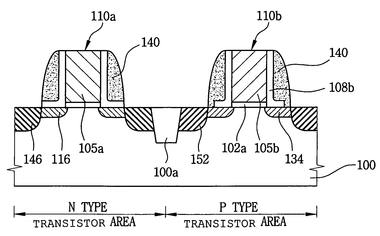
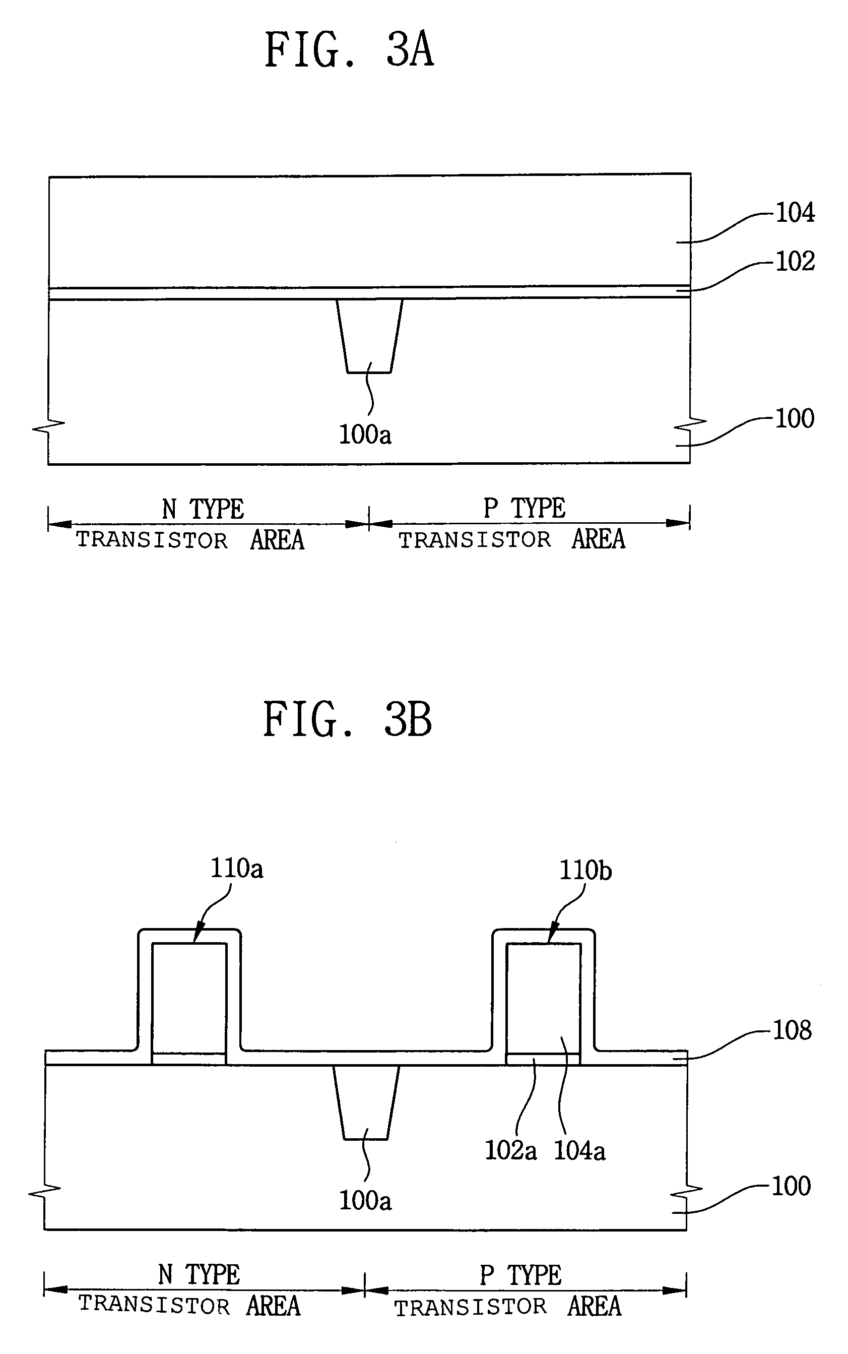
[0023]Referring to FIG. 3A, a semiconductor substrate 100 is divided into an active region and a field region 100a by a trench isolation process. Here, an N type transistor area and a P type transistor area are formed on the semiconductor substrate 100. An N type MOS transistor and a P type MOS transistor are formed on the N type transistor area and the P type transistor area, respectively. Particularly, after a pad oxide layer is formed on the substrate 100, a nitride layer and a high temperature oxide (HTO) ...


PUM


Abstract

A method of manufacturing a transistor of a semiconductor device is provided. The method includes forming an N type gate pattern and a P type gate pattern on a substrate, implanting N type impurities into an N type transistor area, forming an insulation layer on the substrate including the N type gate pattern, forming a first spacer on a sidewall of the P type gate pattern by partially etching the insulation layer in a P type transistor area, and implanting P type impurities into the P type gate pattern and into the P type transistor area, thereby forming a CMOS transistor on the substrate. Thus, damage to the substrate and the transistor is prevented, thereby improving electrical characteristics of the transistor.

Description

CROSS-REFERENCE TO RELATED APPLICATION[0001]This application claims priority to Korean Patent Application No. 2003-15315, filed on Mar. 12, 2003, which is incorporated herein by reference in its entirety.BACKGROUND OF THE INVENTION[0002]1. Technical Field[0003]The present invention relates, generally, to a method of manufacturing a metal oxide semiconductor (MOS) transistor. More particularly, the present invention relates to a method of manufacturing a complementary metal oxide semiconductor (CMOS) transistor having a lightly doped drain (LDD) structure in a semiconductor device.[0004]2. Description of the Related Art[0005]As technologies for manufacturing semiconductor devices have been developed and applications for memory devices have been expanded, memory devices having increased capacities have been required. In particular, integration density of a DRAM device, which includes memory cells composed of one capacitor and one transistor, has been remarkably improved.[0006]A MOS tr...

Claims


Application Information

Patent Timeline
Patent Type & Authority Patents(United States)
IPC IPC(8): H01L21/8238H01L21/425H01L21/336H01L21/8234H01L21/8242H01L27/092
CPCH01L21/82345H01L29/6659H01L29/6656H01L21/823468H01L21/8238
Inventor LEE, DONG-HUNJUNG, JIN-SUK
Owner SAMSUNG ELECTRONICS CO LTD
Why Eureka
Try Eureka