Alignment key structure in a semiconductor device and method of forming the same

a technology of alignment key and semiconductor device, which is applied in the direction of instruments, optics, basic electric elements, etc., can solve the problems of deteriorating the reliability of the semiconductor device, signal noise, and damage to the second metal wiring b>120/b>, so as to prevent damage to the first metal wiring, improve reliability, and enhance productivity

Active Publication Date: 2006-11-02
SAMSUNG ELECTRONICS CO LTD +1
View PDF6 Cites 6 Cited by
  • Summary
  • Abstract
  • Description
  • Claims
  • Application Information

AI Technical Summary

Benefits of technology

[0050] According to the example embodiments of the present invention, a first opening may serve as an alignment key in a wire bonding process to expose a second metal wiring adjacent to a bonding pad. The first opening may have a width substantially narrower than a width of the second metal wiring. Thus, etching damage to the second metal wiring and etching damage to the first metal wiring may be effectively prevented in an etching process for forming the first opening. Additionally, if alignment errors are generated between the first opening and the second metal wiring, the damage to the first metal wiring may be prevented because the first metal wiring may be separated from the first opening. Thus, since the first and the second metal wirings are sufficiently protected during the formation of the first opening, signal noises in a semiconductor device including the first and the second metal wirings are reduced. As a result, the semiconductor device may have improved reliability and enhanced productivity.

Problems solved by technology

However, the second metal wirings 120 can be subject to etch damage during the etching process.
Thus, when the signal lines are exposed through the first opening 132, signal noise may occur as a result of etch damage to the second metal wirings.
The signal noise in turn may then deteriorate the reliability of the semiconductor device.
In addition, since the signal lines have relatively narrower widths than the widths of the power lines or the ground lines, a short or failure of the signal lines may also occur during the etching process.
Furthermore, when etch damage occurs to the second wirings 120, plasma etch damage may also occur in the first metal wirings 110 below the first opening 132 as well, which may in turn lead to further signal noise.

Method used


Image

  • Alignment key structure in a semiconductor device and method of forming the same
  • Alignment key structure in a semiconductor device and method of forming the same
  • Alignment key structure in a semiconductor device and method of forming the same

Examples


Embodiment Construction

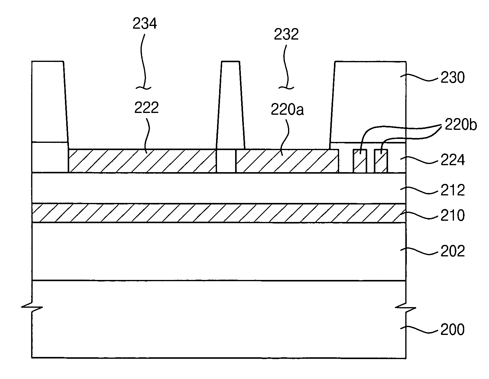
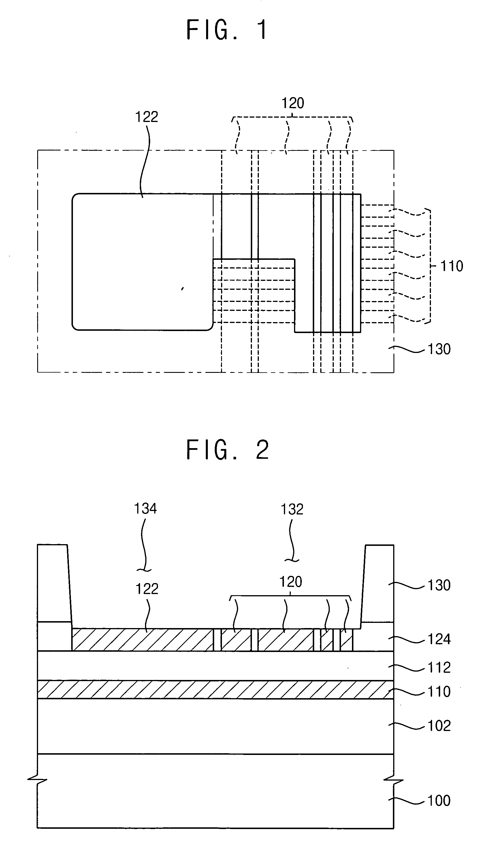
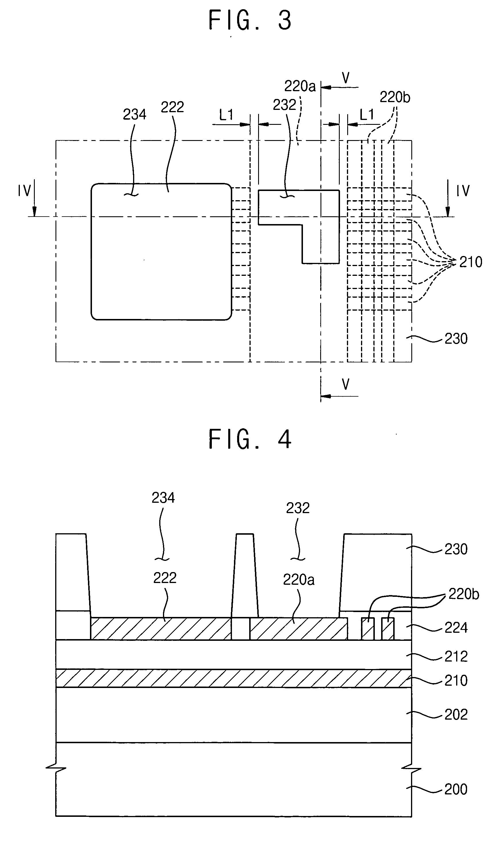
[0062] The present invention is described more fully hereinafter with reference to the accompanying drawings, in which example embodiments of the invention are shown. The present invention may, however, be embodied in many different forms and should not be construed as limited to the embodiments set forth herein. In the drawings, the sizes and relative sizes of layers and regions may be exaggerated for clarity.

[0063] It will be understood that when an element or layer is referred to as being “on”, “connected to” or “coupled to” another element or layer, it can be directly on, connected or coupled to the other element or layer or intervening elements or layers may be present. In contrast, when an element is referred to as being “directly on,”“directly connected to” or “directly coupled to” another element or layer, there are no intervening elements or layers present. Like reference numerals refer to like elements throughout. As used herein, the term “and / or” includes any and all com...


PUM


Abstract

An alignment key structure in a semiconductor device is provided. The alignment key structure includes an insulation layer formed on a substrate, and a passivation layer pattern formed on the insulation layer. The insulation layer includes a plurality of metal wirings. The passivation layer pattern includes a first opening that exposes at least one of the metal wirings. Moreover, the first opening has a width which is narrower than a width of the exposed metal wiring.

Description

CROSS REFERENCE TO RELATED APPLICATION [0001] This application claims priority under 35 USC § 119 to Korean Patent Application No. 2005-36322 filed on Apr. 29, 2005, the contents of which are incorporated by reference herein in its entirety. BACKGROUND OF THE INVENTION [0002] 1. Field of the Invention [0003] The present invention relates to an alignment key structure in a semiconductor device and to a method of manufacturing the same. More particularly, the present invention relates to an alignment key structure employed in a wire bonding process for electrically connecting a bonding pad of a semiconductor device to lead of a lead frame using a conductive line, and to a method of manufacturing the same. [0004] 2. Description of the Related Art [0005] A semiconductor device is generally manufactured by the following processes (i) a fabrication (FAB) process that forms electrical circuits on a semiconductor substrate such as a silicon wafer, (ii) an electrical die sorting (EDS) proces...

Claims


Application Information

Patent Timeline
Patent Type & Authority Applications(United States)
IPC IPC(8): H01L21/8238H01L31/00H01L29/739
CPCH01L23/544H01L2224/05554H01L24/05H01L24/85H01L2223/54473H01L2224/05599H01L2224/05644H01L2224/85121H01L2924/01013H01L2924/01014H01L2924/01022H01L2924/01029H01L2924/01073H01L2924/01074H01L2924/01079H01L2924/01082H01L2924/04941H01L2924/04953H01L2924/05042H01L2924/14H01L2924/19041H01L2924/01019H01L2924/01023H01L2924/01033H01L2924/00014H01L24/03H01L2224/02166H01L2924/10253H01L2924/00H01L2224/48H01L24/45H01L2224/45144H01L2224/45015H01L2924/207G03F9/7076G03F9/708H01L2223/54426
Inventor PARK, SEOK-HANPARK, JOO-SUNGHAN, DONG-HYUN
Owner SAMSUNG ELECTRONICS CO LTD
Why Eureka
Try Eureka