Manufacturing method of semiconductor structure

A manufacturing method and semiconductor technology, applied in semiconductor/solid-state device manufacturing, electrical components, circuits, etc., can solve problems such as poor electrical performance of semiconductor devices, and achieve the effects of improving formation quality, avoiding collapse, and improving electrical performance.

Active Publication Date: 2018-03-09
SEMICON MFG INT (SHANGHAI) CORP +1
View PDF4 Cites 5 Cited by
  • Summary
  • Abstract
  • Description
  • Claims
  • Application Information

AI Technical Summary

Problems solved by technology

[0006] However, even with the introduction of stress layers in the FinFET fabrication...

Method used


Image

  • Manufacturing method of semiconductor structure
  • Manufacturing method of semiconductor structure
  • Manufacturing method of semiconductor structure

Examples


Embodiment Construction

[0015] The electrical performance of the semiconductor device in the prior art is poor, and the reason thereof is analyzed in combination with a manufacturing method of a semiconductor structure. The manufacturing method of described semiconductor structure comprises the following steps:

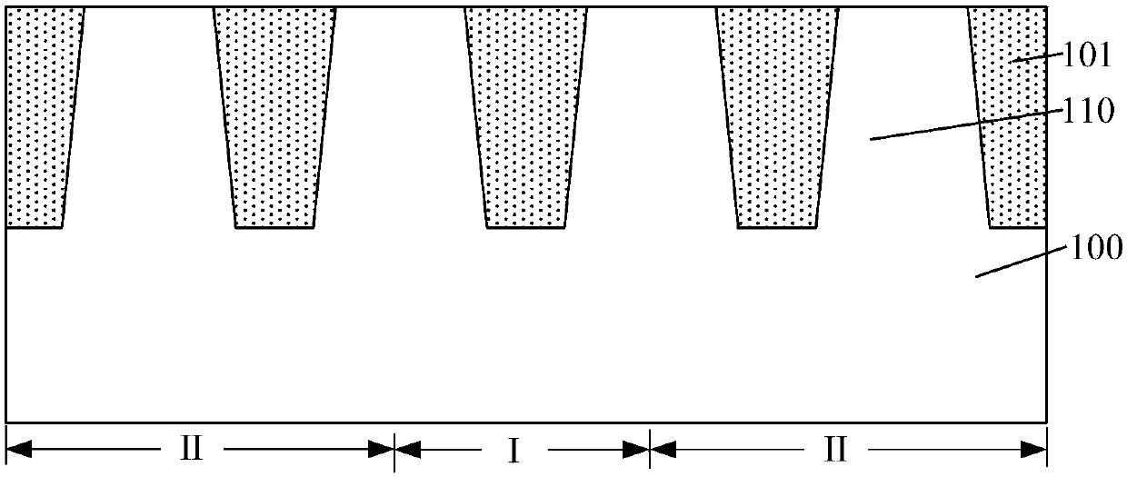
[0016] refer to figure 1 , providing a substrate 100 and discrete fins 110 on the substrate 100, the substrate 100 includes a first region I and a second region II, the density of fins 110 in the first region I is greater than that in the second region Fin 110 density in region II.

[0017] continue to refer figure 1 , forming an initial isolation layer 101 on the substrate 100 between the fins 110 , the top of the initial isolation layer 101 is flush with the top of the fins 110 .

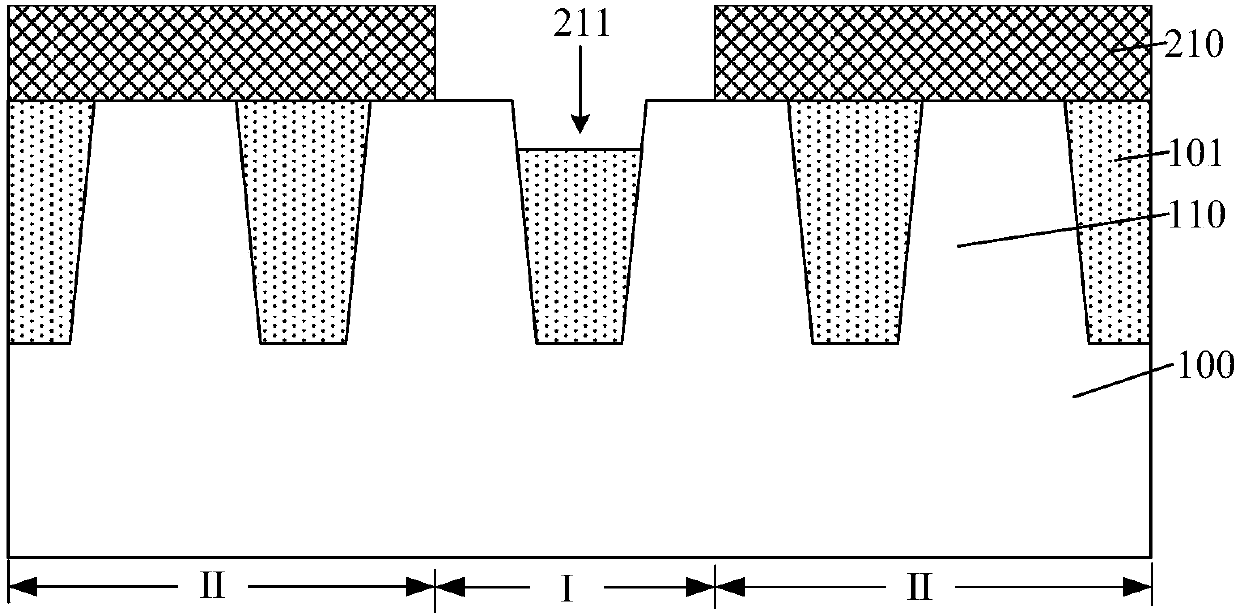
[0018] refer to figure 2 A patterned hard mask layer 210 is formed on top of the fins 110 and the initial isolation layer 101 in the second region II, and the hard mask layer 210 has the initial isolation...


PUM


Abstract

The invention relates to a manufacturing method of a semiconductor structure. The method includes the following steps that: a substrate and discrete fins on the substrate are provided, the extending direction of the fins is a first direction, and a direction perpendicular to the first direction is a second direction; an initial isolation layer between the fins is formed on the substrate and includes a first initial isolation layer for achieving the isolation of the fins in the first direction; part of the first initial isolation layer is removed by a certain thickness, so that a first isolation layer is formed, and the top of the first isolation layer is lower than the tops of the fins, and a trench is formed between the fins; a second isolation layer filling the trench is formed; protective sidewalls are formed on the sidewalls of the second isolation layer which are higher than the tops of the fins; and part of a second initial isolation layer and the second isolation layer are removed by a certain thickness. According to the manufacturing method of the semiconductor structure of the invention, the protective sidewalls are formed on the sidewalls of the second isolation layer which are higher than the tops of the fins, and therefore, when part of the second isolation layer is removed by a certain thickness, the protective sidewalls can protect the sidewalls of the second isolation layer, and therefore, the problem of the formation of protrusion defects of the second isolation layer because of insufficient lateral etching can be avoided.

Description

technical field [0001] The invention relates to the field of semiconductors, in particular to a method for manufacturing a semiconductor structure. Background technique [0002] With the continuous development of semiconductor process technology, the development trend of semiconductor process nodes following Moore's Law continues to decrease. In order to adapt to the reduction of the process node, the channel length of the MOSFET field effect tube has to be shortened. The shortening of the channel length has the advantages of increasing the die density of the chip and increasing the switching speed of the MOSFET field effect tube. [0003] However, as the channel length of the device is shortened, the distance between the source and the drain of the device is also shortened, so that the control ability of the gate to the channel becomes worse, resulting in the phenomenon of subthreshold leakage, namely So-called short-channel effects (SCE: short-channel effects) are more l...

Claims


Application Information

Patent Timeline
IPC IPC(8): H01L21/8234
CPCH01L21/823431H01L21/823481
Inventor 周飞
Owner SEMICON MFG INT (SHANGHAI) CORP
Why Eureka
Try Eureka