Semiconductor structures and methods of forming them

A semiconductor and work function layer technology, which is applied in semiconductor/solid-state device manufacturing, transistors, electrical components, etc., can solve the problems that the electrical properties of semiconductor structures need to be improved, so as to avoid undercut area defects, shorten the etching time, and improve the quality of side walls. good shape effect

Active Publication Date: 2020-10-09
SEMICON MFG INT (SHANGHAI) CORP +1
View PDF7 Cites 0 Cited by
  • Summary
  • Abstract
  • Description
  • Claims
  • Application Information

AI Technical Summary

Problems solved by technology

[0004] Although the introduction of high-k metal gates can improve the electrical properties of semiconductor structures to a certain extent, the electrical properties of semiconductor structures formed by existing technologies still need to be improved.

Method used


Image

  • Semiconductor structures and methods of forming them
  • Semiconductor structures and methods of forming them
  • Semiconductor structures and methods of forming them

Examples


Embodiment Construction

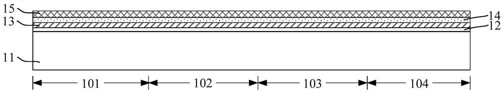
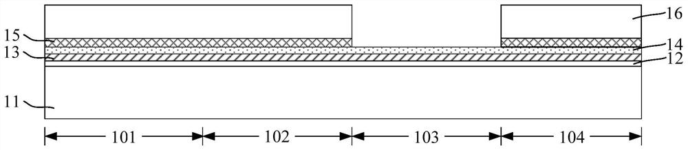
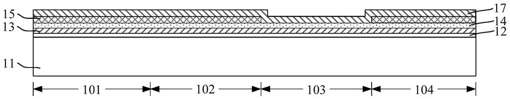
[0031]It can be seen from the background art that the electrical performance of the semiconductor structure formed in the prior art needs to be improved. Especially when the semiconductor structure includes P-type devices with different threshold voltages (Threshold Voltage) and N-type devices with different threshold voltages, the problem of poor electrical performance of the semiconductor structure is particularly significant.

[0032] In order to meet the requirements of NMOS tube and PMOS tube to improve the threshold voltage, different metal materials are usually used as the material of the work function (WF, Work Function) layer in the gate structure of the NMOS tube and the PMOS tube, and the work function layer in the NMOS tube The material may be referred to as an N-type work function material, and the work function layer material in the PMOS transistor may be referred to as a P-type work function material. When the NMOS transistor and the PMOS transistor share the sa...


PUM

PropertyMeasurementUnit
thicknessaaaaaaaaaa
thicknessaaaaaaaaaa
electron work functionaaaaaaaaaa

Abstract

The invention relates to a semiconductor structure and a formation method thereof. The formation method comprises the steps of providing a substrate, wherein the substrate comprises a first N region,a second N region, a first P region and a second P region, and the first N region is adjacent to the first P region; forming a blocking layer on a grid dielectric layer; forming a first work functionlayer on the blocking layer; etching the first work function layer, and reserving the first work function layer arranged on the first P region; forming second work function layers on the first N region, the first P region, the second N region and the second P region; etching the second work function layers on the first N region and the second N region until the grid dielectric layer of the first Nregion is exposed; forming a third work function layer, wherein the third work function layer also covers a side wall of the blocking layer at a junction of the first N region and the first P region,a side wall of the first work function layer and a side wall of the second work function layer; and forming a fourth work function layer on the third work function layer. By the formation method, thefirst work function layer and the second work function layer of the first P region are prevented from being horizontally etched, and the electrical property of the formed semiconductor structure is improved.

Description

technical field [0001] The invention relates to the technical field of semiconductor manufacturing, in particular to a semiconductor structure and a forming method thereof. Background technique [0002] The main semiconductor device of an integrated circuit, especially a very large scale integrated circuit, is a metal-oxide-semiconductor field effect transistor (MOS transistor). With the continuous development of integrated circuit manufacturing technology, the technology nodes of semiconductor devices are continuously reduced, and the geometric dimensions of semiconductor structures are continuously reduced following Moore's law. When the size of the semiconductor structure is reduced to a certain extent, various secondary effects caused by the physical limit of the semiconductor structure appear one after another, and it becomes more and more difficult to scale down the feature size of the semiconductor structure. Among them, in the field of semiconductor manufacturing, t...

Claims


Application Information

Patent Timeline
Patent Type & Authority Patents(China)
IPC IPC(8): H01L21/8238H01L27/092
CPCH01L21/823857H01L27/092
Inventor 李勇
Owner SEMICON MFG INT (SHANGHAI) CORP
Why Eureka
Try Eureka