A processing method for monolithic integration of micro-mechanical structure and integrated circuit

A micro-mechanical structure and integrated circuit technology, applied in micro-structure technology, micro-structure devices, manufacturing micro-structure devices, etc., can solve problems such as affecting device reliability, easy generation of residues on the sidewalls of isolation grooves, affecting processing yields, etc. , to avoid the effect of lateral etching

Inactive Publication Date: 2014-10-08
PEKING UNIV
View PDF4 Cites 0 Cited by
  • Summary
  • Abstract
  • Description
  • Claims
  • Application Information

AI Technical Summary

Problems solved by technology

However, this method also has defects: when the silicon isotropic etching method is used to remove the single crystal silicon in the air isolation groove, a part of the MEMS device structure will also be etched laterally; on the other hand, dielectric materials such as silicon oxide The floating electrodes made of metal and metal have a large stress, which will affect the reliability of the device
However, during the process of anisotropic etching of the MEMS structure, residues are likely to be generated on the side walls of the isolation trenches that have been processed, which affects the processing yield.

Method used


Image

  • A processing method for monolithic integration of micro-mechanical structure and integrated circuit
  • A processing method for monolithic integration of micro-mechanical structure and integrated circuit
  • A processing method for monolithic integration of micro-mechanical structure and integrated circuit

Examples


Embodiment Construction

[0019] The present invention will be described in detail below in conjunction with the accompanying drawings and embodiments.

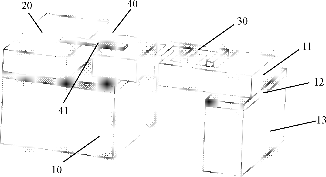
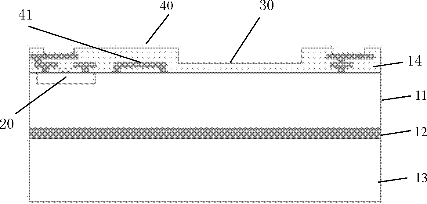
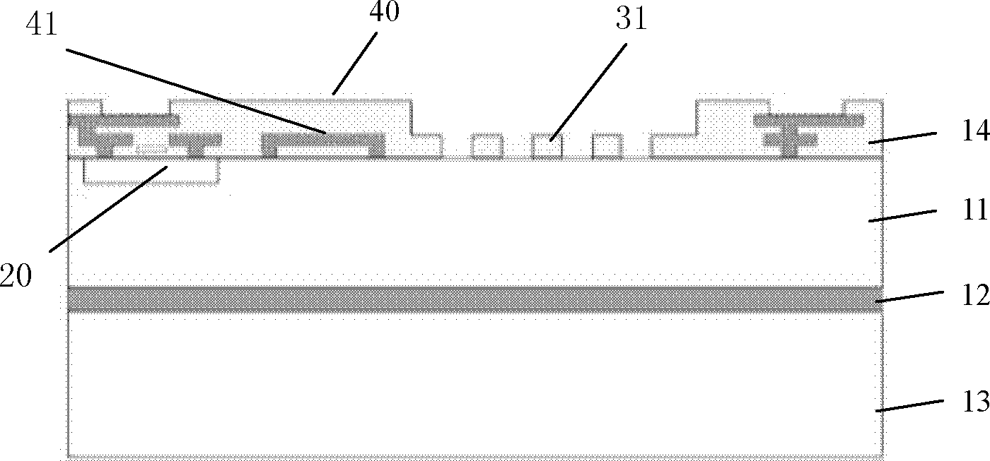
[0020] Such as figure 1 As shown, the present invention integrates and processes MEMS devices on an SOI substrate 10 . The SOI substrate 10 includes a single crystal silicon device layer 11 , a silicon dioxide buried oxide layer 12 and a single crystal silicon substrate layer 13 . The device layer 11 is divided into an integrated circuit area 20 and a MEMS structure area 30 , and an isolation area 40 for separating the integrated circuit area 20 and the MEMS structure area 30 . The silicon in the isolation region 40 is removed to form an isolation groove, so that the silicon structures corresponding to the integrated circuit region 20 and each MEMS structure region 30 are independent from each other to realize electrical isolation. The integrated circuit region 20 and the silicon structures corresponding to each MEMS structure region 30 are mechanic...


PUM


Abstract

The invention relates to a micromechanical structure and integrated circuit monolithic integrated processing method which comprises the following steps of dividing the device layer of the substrate of an SOI (silicon on insulator) into an integrated circuit region, an MEMS structural region and an isolation region; adopting a standard integrated circuit processing method to process an integrated circuit in the integrated circuit region and arranging an electrode striding the isolation region; defining an MEMS structural pattern on the surface of a dielectric layer produced on the surface of the device layer during the processing of the integrated circuit, carrying out mechanical erosion, and obtaining the MEMS structure mask formed by the dielectric layer; then carrying out silicon anisotropy mechanical erosion on the device layer according to the MEMS structure mask so as to obtain the MEMS structure; performing the filling protection on the clearance in the MEMS structure, then carrying out mechanical erosion to the dielectric layer in the isolation region; and taking light-sensitive lacquer and the electrode at the isolation region as masks, and carrying out silicon anisotropy mechanical erosion and silicon isotropy mechanical erosion to the device layer of the isolation region. The invention meets the precondition of foundry manufacturing of integrated circuits, and has higher finished product processing rate.

Description

technical field [0001] The invention relates to a method for processing an integrated chip, in particular to a method for monolithically integrating a micromechanical structure and an integrated circuit. Background technique [0002] Capacitive sensors such as inertial sensors implemented by Microelectromechanical Systems (MEMS) technology have the advantages of small size, light weight and low cost, and have broad application prospects in the fields of military, automobile industry and consumer electronics. Limited by size, MEMS sensor signals are generally weak and easily affected by parasitic capacitance. Integrating the MEMS sensor header structure and the signal processing circuit on the same chip can effectively reduce the adverse effects of parasitic effects, and at the same time reduce the device volume and reduce manufacturing costs. It is one of the important directions for the development of MEMS technology. To complete the processing of integrated circuits and M...

Claims


Application Information

Patent Timeline
Patent Type & Authority Patents(China)
IPC IPC(8): B81C1/00
Inventor 杨振川闫桂珍郝一龙
Owner PEKING UNIV
Why Eureka
Try Eureka