Semiconductor device and forming method thereof

A semiconductor and device technology, applied in the field of semiconductor devices and their formation, can solve problems such as poor performance of semiconductor devices, and achieve the effect of improving performance

Active Publication Date: 2019-12-31
SEMICON MFG INT (SHANGHAI) CORP +1
View PDF6 Cites 0 Cited by
  • Summary
  • Abstract
  • Description
  • Claims
  • Application Information

AI Technical Summary

Problems solved by technology

[0004] However, before the epitaxial process is used to form the source and drain regions, an epitaxial cleaning process is usually performed to completely remove impurities on the substrate surface. The epitaxial cleaning process will cause over-etching of the oxide layer on the substrate surface, resulting in the subsequent formation of semiconductor poor device performance

Method used


Image

  • Semiconductor device and forming method thereof
  • Semiconductor device and forming method thereof
  • Semiconductor device and forming method thereof

Examples


Embodiment Construction

[0030] As mentioned in the background, the performance of semiconductor devices formed in the prior art needs to be improved.

[0031] Figure 1 to Figure 5 It is a structural schematic diagram of an embodiment of the forming process of a fin field effect transistor.

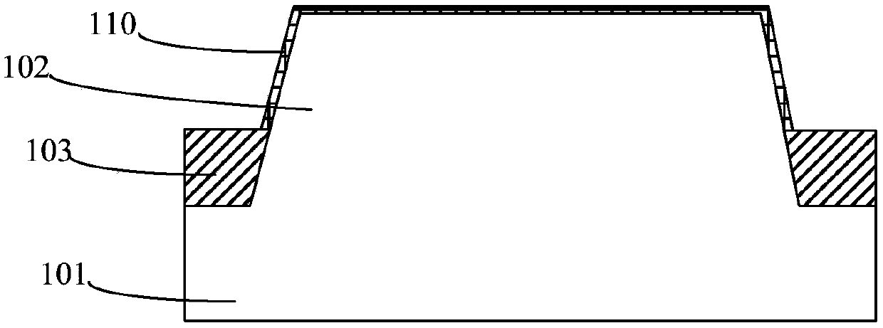
[0032] Please refer to figure 1 , providing a base 101, the base surface has a fin 102, the base surface has an isolation layer 103, the top surface of the isolation layer 103 is lower than the top surface of the fin 102, and the isolation layer 103 covers the Part of the sidewall of the fin portion 102 ; a dummy gate dielectric layer 110 is formed on the sidewall and top surface of the fin portion 102 .

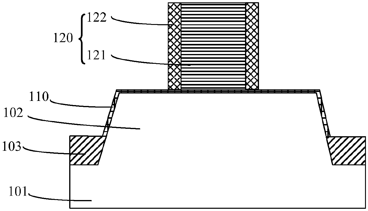
[0033] Please refer to figure 2 , forming a dummy gate structure 120 on the dummy gate dielectric layer 110, the dummy gate structure 120 includes a dummy gate electrode layer 121 and sidewalls 122 located on the sidewalls of the dummy gate electrode layer; the dummy gate structure 120 across the fin port...


PUM


Abstract

The invention discloses a semiconductor device and a forming method thereof. The method comprises the steps: providing a substrate, wherein the substrate has a pseudo-gate dielectric film; forming a pseudo-gate structure on the pseudo-gate dielectric film, wherein the pseudo-gate structure comprises a pseudo-gate electrode layer and sacrifice side walls located on the side walls of the pseudo-gateelectrode layer; removing a part of the pseudo-gate dielectric film at the two sides of the pseudo-gate structure until the surface of the substrate is exposed, and forming a pseudo-gate dielectric layer at the bottom of the pseudo-gate structure; after the pseudo-gate dielectric layer is formed, removing the sacrifice side walls; after the sacrifice side walls are removed, forming a side wall structure on the side wall of the pseudo-gate electrode layer and the side wall of the pseudo-gate dielectric layer; and forming openings in the substrate at the two sides of the pseudo-gate electrode layer and the side wall structure. The semiconductor device formed by the method is good in performance.

Description

technical field [0001] The invention relates to the field of semiconductor manufacturing, in particular to a semiconductor device and a forming method thereof. Background technique [0002] With the rapid development of integrated circuit manufacturing technology, the size of semiconductor devices in the integrated circuit is continuously reduced, so that the operation speed of the entire integrated circuit will be effectively improved. However, when the size of the device is further reduced, in the case of a fin field effect transistor, the resistance and parasitic resistance of the gate and source / drain will increase accordingly, which will reduce the overall effect of the device reduction. Improvement of circuit performance is hindered. [0003] At present, the industry applies the selective epitaxial growth process to the semiconductor process to overcome the above-mentioned problems. [0004] However, before the epitaxial process is used to form the source and drain r...

Claims


Application Information

Patent Timeline
Patent Type & Authority Applications(China)
IPC IPC(8): H01L21/336H01L29/78H01L29/423
CPCH01L29/785H01L29/66545H01L29/66795H01L29/42364
Inventor 周飞
Owner SEMICON MFG INT (SHANGHAI) CORP
Why Eureka
Try Eureka