Display panel manufacturing method and display panel

A technology for display panels and manufacturing methods, applied in the fields of instruments, nonlinear optics, optics, etc., which can solve problems such as long etching time, reduced production capacity, and difficulty in controlling the organic flat layer

Pending Publication Date: 2022-08-09
SHENZHEN CHINA STAR OPTOELECTRONICS SEMICON DISPLAY TECH CO LTD
View PDF3 Cites 0 Cited by
  • Summary
  • Abstract
  • Description
  • Claims
  • Application Information

AI Technical Summary

Problems solved by technology

[0004] The embodiment of the present application provides a method for manufacturing a display panel and a display panel, which can solve the problem that it is difficult to control the formation of an organic planar layer with a predetermined thickness, and the resulting waste of materials, long etching time, and reduced production capacity

Method used


Image

  • Display panel manufacturing method and display panel
  • Display panel manufacturing method and display panel
  • Display panel manufacturing method and display panel

Examples


Embodiment 1

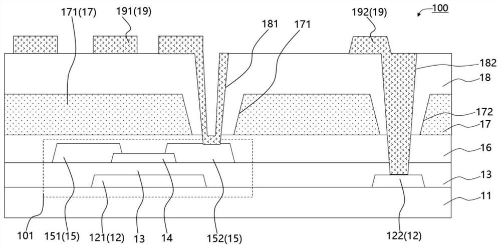
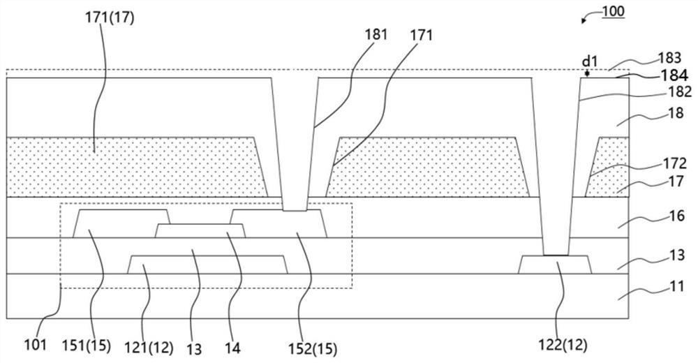
[0047] see Figure 1 to Figure 3 , figure 1 A first schematic flowchart of a method for manufacturing a display panel provided by an embodiment of the present application; figure 2A schematic cross-sectional structure diagram of a partial structure of a display panel provided in an embodiment of the present application, image 3 This is a schematic diagram of an intermediate process of a method for manufacturing a display panel according to an embodiment of the present application.

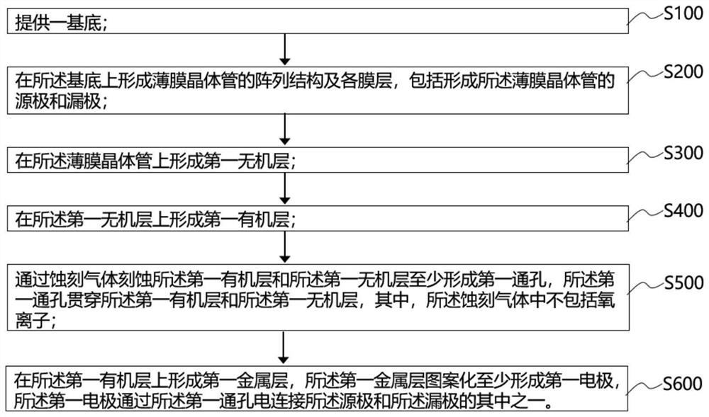
[0048] An embodiment of the present application provides a method for manufacturing a display panel, including: providing a substrate; forming an array structure of thin film transistors and each film layer on the substrate, including forming a source electrode and a drain electrode of the thin film transistor; forming on the thin film transistor a first inorganic layer; a first organic layer is formed on the first inorganic layer; at least a first through hole is formed by etching the first or...

Embodiment 2

[0071] This embodiment is the same as or similar to the above-mentioned embodiment, and the differences further describe the features of the manufacturing method of the display panel.

[0072] see Figure 4 , Figure 4 This is a second schematic flow chart of a method for manufacturing a display panel provided in an embodiment of the present application.

[0073] In some embodiments, when at least the first through hole is formed by etching the first organic layer and the first inorganic layer with an etching gas, the etching gas includes fluorine ions.

[0074] Specifically, in step S500, when at least the first through holes 181 are formed by etching the first organic layer 18 and the first inorganic layer 16 with an etching gas, the etching gas includes fluorine ions.

[0075] Specifically, the etching gas contains fluorine ions, and the etching gas may include nitrogen trifluoride (NF3), carbon tetrafluoride (CF4), and the like.

[0076] Specifically, the etching gas co...

Embodiment 3

[0084] This embodiment is the same as or similar to the above-mentioned embodiment, and the differences further describe the features of the manufacturing method of the display panel.

[0085] see Figure 5 , Figure 5 A third schematic flow diagram of a method for manufacturing a display panel provided in an embodiment of the present application.

[0086] In some embodiments, further comprising between forming the first inorganic layer on the array structure of the thin film transistor and forming the first organic layer on the first inorganic layer: forming a color blocking layer on the first inorganic layer; wherein, When the first organic layer is formed on the first inorganic layer, the first organic layer is formed on the color resist layer; wherein, when at least the first through hole is formed by etching the first organic layer and the first inorganic layer with an etching gas, the first organic layer is formed on the color resist layer. A through hole also penetrat...


PUM


Abstract

The embodiment of the invention discloses a manufacturing method of a display panel and the display panel, and the method comprises the steps: forming an array structure of a thin film transistor and each film layer on a substrate, and forming a source electrode and a drain electrode of the thin film transistor; forming a first inorganic layer on the thin film transistor; forming a first organic layer on the first inorganic layer; the first organic layer and the first inorganic layer are etched through etching gas, at least a first through hole is formed, the first through hole penetrates through the first organic layer and the first inorganic layer, and the etching gas does not comprise oxygen ions; a first metal layer is formed on the first organic layer, the first metal layer is patterned to at least form a first electrode, and the first electrode is electrically connected with one of the source electrode and the drain electrode through the first through hole. According to the method, the oxygen ions are removed in the etching gas, the oxygen ions are reduced or prevented from transversely etching the first organic layer, and the thickness of the first organic layer is not reduced when the first through hole is formed, so that the first organic layer with the preset thickness is easily controlled to be formed.

Description

technical field [0001] The present application relates to the field of display, and in particular, to a manufacturing method of a display panel and a display panel. Background technique [0002] With the development of display technology, display panels have been widely used in people's lives, such as display screens of mobile phones and computers. In the manufacturing process of display panels, especially in the manufacturing process of COA (color filter on array) type liquid crystal display panels, it is necessary to introduce an organic film layer such as PFA (Polymer Film on Array). The functions of flat array substrate, reduction of parasitic capacitance and improvement of aperture ratio, etc. [0003] However, when the through hole is formed by etching in the organic flat layer, the etching gas will laterally etch the organic flat layer, so that the thickness of the organic flat layer is greatly reduced. Therefore, it is difficult to control the formation of a predete...

Claims


Application Information

Patent Timeline
Patent Type & Authority Applications(China)
IPC IPC(8): G02F1/1333G02F1/1362
CPCG02F1/1333G02F1/1362G02F1/136222
Inventor 吴灵智张忠阳刘忠杰任武峰郭雷
Owner SHENZHEN CHINA STAR OPTOELECTRONICS SEMICON DISPLAY TECH CO LTD
Why Eureka
Try Eureka