Nitride semiconductor device and manufacturing method thereof

a semiconductor and nitride technology, applied in the direction of semiconductor devices, basic electric elements, electrical apparatus, etc., can solve the problems of difficult to achieve excellent device characteristics, unavoidable damage to the surface of the algan layer due to etching, etc., to improve the morphology of the surface of the electron supply layer, improve the stability of the surface, and improve the effect of surface morphology

Active Publication Date: 2016-03-22
ROHM CO LTD
View PDF10 Cites 5 Cited by
  • Summary
  • Abstract
  • Description
  • Claims
  • Application Information

AI Technical Summary

Benefits of technology

[0009]One object of the present invention is to provide a nitride semiconductor device having an excellent boundary between the nitride semiconductor and the gate insulating film, thus improving the device characteristics, and a manufacturing method therefor.
[0028]A twelfth aspect of the present invention is the method of the eleventh aspect, wherein the step of forming an opening in the passivation film includes etching, using the gate insulating film as an etching stopper. With this method, when an opening is formed in the passivation film, the surface of the electron supply layer directly below the gate electrode is not exposed, and thus, etching damage on the surface of the electron supply layer can be prevented, and the exposure of the electron supply layer to air can also be avoided. As a result, a nitride semiconductor device with excellent characteristics can be manufactured.

Problems solved by technology

As a result, damage to the surface of the AlGaN layer due to etching is unavoidable.
Thus, the boundary between the AlGaN layer and the gate insulating layer is not necessarily in a good state, which presents a problem in that it is difficult to attain excellent device characteristics.

Method used


Image

  • Nitride semiconductor device and manufacturing method thereof
  • Nitride semiconductor device and manufacturing method thereof
  • Nitride semiconductor device and manufacturing method thereof

Examples


embodiment 1

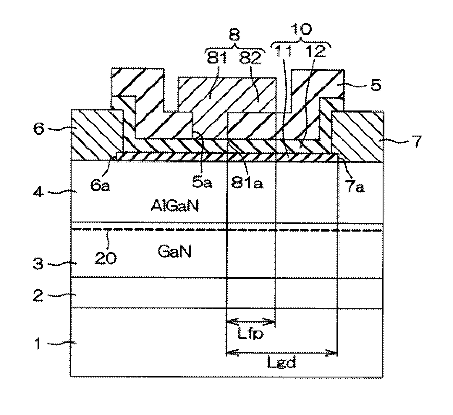
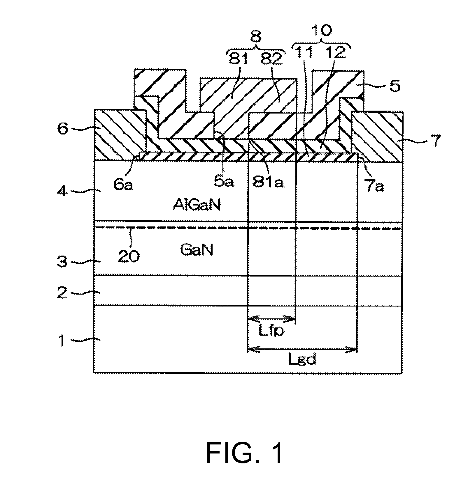
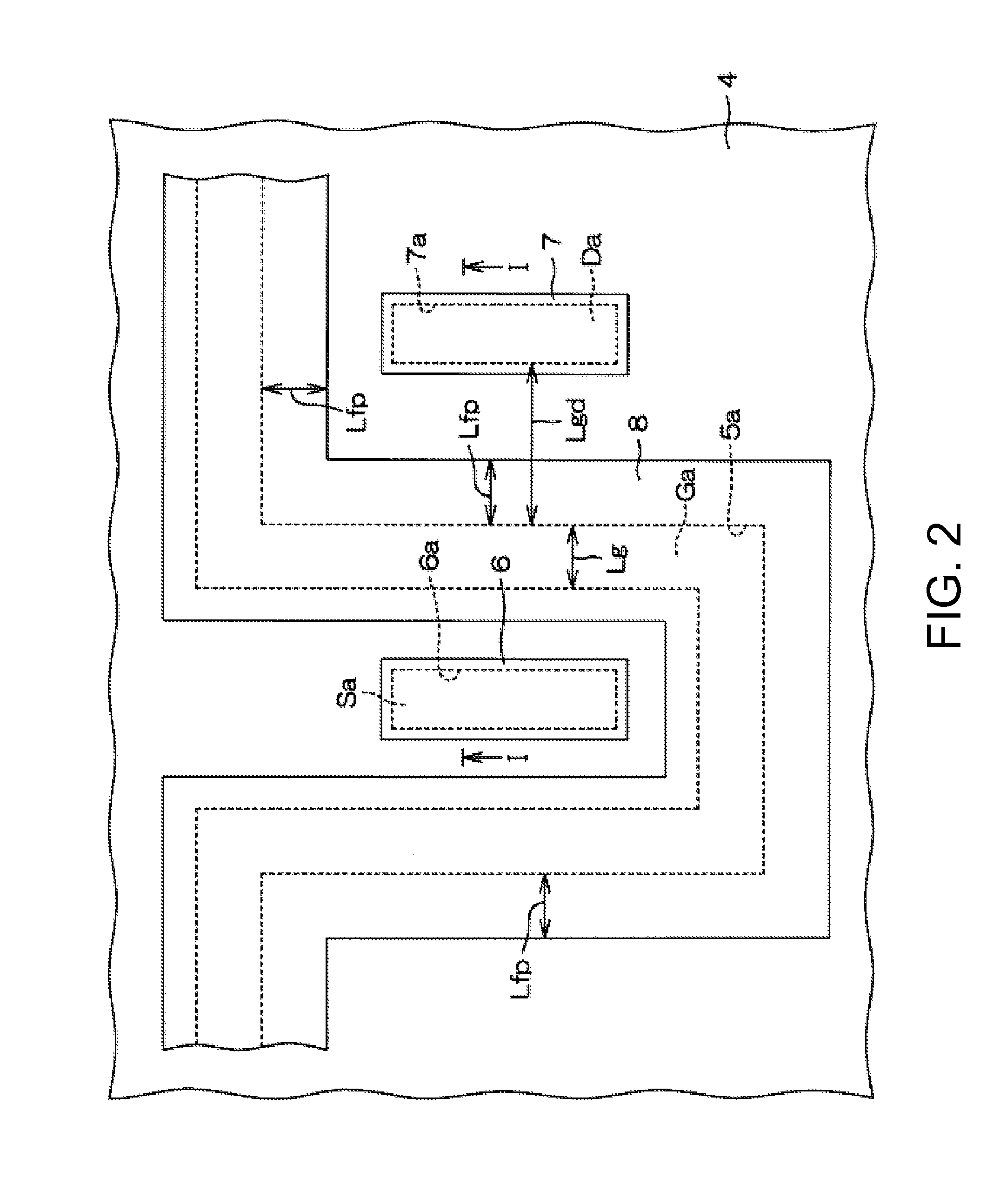
[0045]FIG. 1 is a cross-sectional view for describing a configuration of a nitride semiconductor device of the present invention. FIG. 2 is a plan view of the nitride semiconductor device. FIG. 1 shows a cross-section of FIG. 2 along the line I-I. The nitride semiconductor device includes a substrate 1 (a silicon substrate, for example), a buffer layer 2 formed on a surface of the substrate 1, an electron transport layer 3 formed on the buffer layer 2 by epitaxial growth, and an electron supply layer 4 formed on the electron transport layer 3 by epitaxial growth. The nitride semiconductor device further includes a gate insulating film 10 (not shown in FIG. 2) covering the surface of the electron supply layer 4, a passivation film 5 (not shown in FIG. 2) covering the gate insulating film 10, and a source electrode 6 and a drain electrode 7, which are ohmic electrodes in ohmic contact with the electron supply layer 4 through contact holes 6a and 7a formed in the gate insulating film ...

embodiment 2

[0075]FIG. 4 is a schematic cross-sectional view for describing a configuration of a nitride semiconductor device of the present invention. In FIG. 4, portions corresponding to the portions in FIG. 1 are assigned the same reference characters.

[0076]In the present embodiment, an electron supply layer 4 includes a second layer 42 as a cap layer formed on a first layer 41 that is made of AlGaN. A source electrode 6 and a drain electrode 7, which are ohmic electrodes, and a gate insulating film 10 are formed on the second layer 42, in contact therewith.

[0077]The second layer 42 is made of GaN, which is a nitride semiconductor of the same composition as an electron transport layer 3, and the thickness thereof is between 2 nm and 16 nm inclusive (more preferably 8 nm or less).

[0078]The second layer 42 functioning as a cap layer contributes to an improved surface morphology of the electron supply layer 4. In other words, on the surface of the electron transport layer 3 made of GaN, the fi...


PUM

PropertyMeasurementUnit
thicknessaaaaaaaaaa
thicknessaaaaaaaaaa
thicknessaaaaaaaaaa

Abstract

Provided are a nitride semiconductor device having an excellent boundary between a nitride semiconductor and a gate insulating film, resulting in improved device characteristics, and a manufacturing method therefor. The nitride semiconductor device includes: an electron transport layer made of a nitride semiconductor; an electron supply layer layered on the electron transport layer, the electron supply layer being made of a nitride semiconductor including Al and having an Al composition different from that of the electron transport layer; a source electrode and a drain electrode formed on the electron supply layer with a gap therebetween; a gate insulating film covering the surface of the electron supply layer between the source electrode and the drain electrode; a passivation film covering a surface of the gate insulating film and having an opening between the source electrode and the drain electrode; and a gate electrode having a main gate body in the opening facing the electron supply layer through the gate insulating film.

Description

[0001]This application claims the benefit of Japanese Application No. 2012-118826, filed in Japan on May 24, 2012, which is hereby incorporated by reference in its entirety.BACKGROUND OF THE INVENTION[0002]1. Field of the Invention[0003]The present invention relates to a semiconductor device made of a group III nitride semiconductor (sometimes referred to simply as a “nitride semiconductor” below) and a manufacturing method therefor.[0004]2. Description of Related Art[0005]A group III nitride semiconductor is a semiconductor that uses nitrogen as the group V element in a group III-V semiconductor. Aluminum nitride (AlN), gallium nitride (GaN), and indium nitride (InN) are representative examples thereof. In general, it is possible to express this as AlXInYGa1-X-YN (0≦X≦1, 0≦Y≦1, 0<X+Y<1).[0006]A MISFET (metal-insulator-semiconductor field effect transistor) using such a nitride semiconductor is proposed. Patent Document 1 discloses one example of such a MISFET. The MISFET disc...

Claims


Application Information

Patent Timeline
Patent Type & Authority Patents(United States)
IPC IPC(8): H01L29/66H01L29/78H01L29/778H01L29/51H01L29/43H01L29/20
CPCH01L29/78H01L29/513H01L29/517H01L29/518H01L29/66462H01L29/66477H01L29/7786H01L29/2003H01L29/432
Inventor AKUTSU, MINORUFUJIWARA, TETSUYA
Owner ROHM CO LTD
Why Eureka
Try Eureka