Power device with improved edge termination

a power device and edge termination technology, applied in the direction of semiconductor devices, diodes, electrical apparatus, etc., can solve the problems of high resistivity, breakdown voltage performance, high power loss of conventional devices,

Active Publication Date: 2009-04-21
SEMICON COMPONENTS IND LLC
View PDF5 Cites 45 Cited by
  • Summary
  • Abstract
  • Description
  • Claims
  • Application Information

AI Technical Summary

Problems solved by technology

For example, in the mid to high voltage range (i.e., 60 to 2,000 volts), a conventional device suffers from high resistivity, since the drift region needs to be lightly doped in order for the device to sustain high voltages during the blocking state.
The high resistivity of the drift region results in higher source-to-drain on-resistance RDSon, which in turn results in high power losses.
Because of the inverse relationship between RDSon and the breakdown voltage, improving the breakdown voltage performance of the device while maintaining a low RDSon poses a challenge.
However, one problem with the design of charge balance devices is the edge termination area.
It is a challenge to achieve charge balance at the interface between the active region and the termination region since an opposing junction to couple to the last active cell can be difficult to implement.
If all the active cells are identically charge balanced except at the active to termination interface region, then this interface region becomes the limiting factor in achieving high breakdown voltage.
The edge termination breakdown at low current levels does not hinder device performance however, during high current avalanche events such as unclamped inductive load (UIL) switching, the limited area of the termination region relative to the active array cannot handle the power losses.
This detrimentally impacts the safe operating area (SOA) of the device.

Method used


Image

  • Power device with improved edge termination
  • Power device with improved edge termination
  • Power device with improved edge termination

Examples


Embodiment Construction

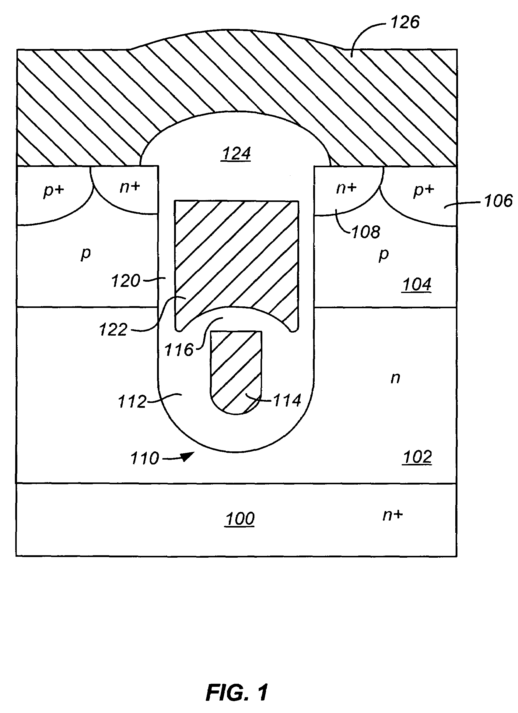
[0027]Embodiments of the present invention address the above problems and other problems by providing structures and methods that limit the current in the termination area during a UIL switching event. A resistive voltage division technique is employed in the termination region which reduces the amount of current that flows through the edge termination region during a high avalanche current event by progressively shifting an increasing percentage of the avalanche current from the edge termination region to the active cells. This technique minimizes power dissipation during UIL switching at the edge termination region and improves the SOA performance.

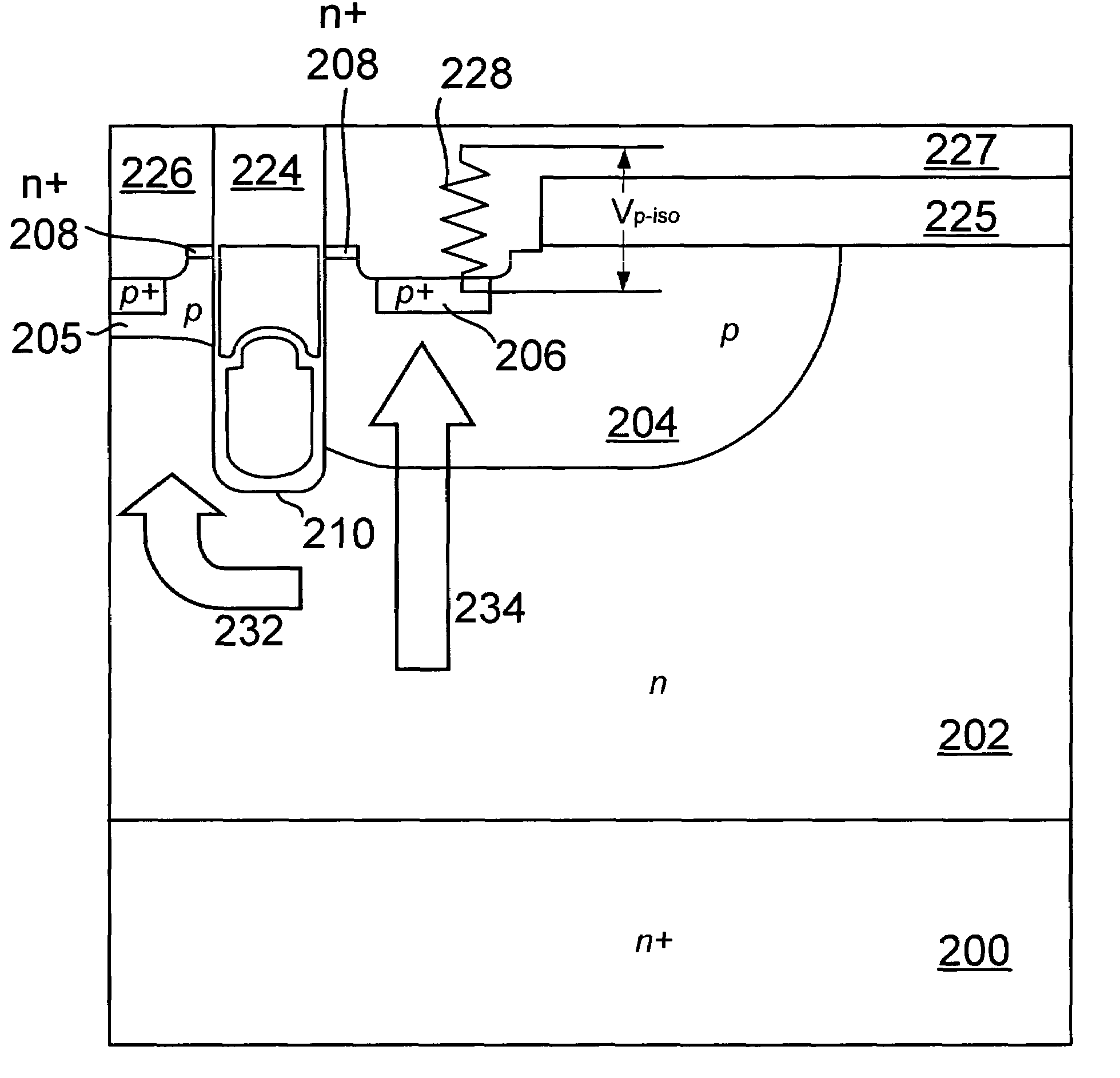
[0028]FIG. 1 shows a simplified cross sectional view of a shielded gate trench MOSFET. For simplicity, embodiments of the invention will be discussed with respect to a shielded gate trench MOSFET as the one shown in FIG. 1. However, the invention is not limited to shielded gate trench MOSFETs. Various conventional power devices, includin...


PUM


Abstract

A field effect transistor includes an active region and a termination region surrounding the active region. A resistive element is coupled to the termination region, wherein upon occurrence of avalanche breakdown in the termination region an avalanche current starts to flow in the termination region, and the resistive element is configured to induce a portion of the avalanche current to flow through the termination region and a remaining portion of the avalanche current to flow through the active region.

Description

CROSS-REFERENCES TO RELATED APPLICATIONS[0001]This application is related to the commonly assigned U.S. application Ser. No. 11 / 026,276, filed Dec. 29, 2004, which disclosure is incorporated herein by reference in its entirety for all purposes.BACKGROUND OF THE INVENTION[0002]The present invention relates to power device technology, and more particularly to improved edge termination for charge balance power devices.[0003]The charge balance concept is a promising evolution in the power device technology. Some of the defining performance characteristics for the power switch are its on-resistance, breakdown voltage and switching speed. Depending on the requirements of a particular application, a different emphasis may be placed on each of these performance criteria. For example, in the mid to high voltage range (i.e., 60 to 2,000 volts), a conventional device suffers from high resistivity, since the drift region needs to be lightly doped in order for the device to sustain high voltages...

Claims


Application Information

Patent Timeline
Patent Type & Authority Patents(United States)
IPC IPC(8): H01L29/00
CPCH01L29/7803H01L29/7808H01L29/7811H01L29/7813H01L29/0646H01L29/0653H01L29/1095H01L29/402H01L29/407H01L29/41741H01L29/456H01L29/00
Inventor YILMAZ, HAMZACALAFUT, DANIEL
Owner SEMICON COMPONENTS IND LLC
Why Eureka
Try Eureka