Scalable electrically eraseable and programmable memory

a programmable memory and programmable memory technology, applied in the field of electrically eraseable and programmable memory (eeprom) cells, can solve the problems of difficult yield management, complicated memory operation, and complex process necessary to fabricate eeprom memories

Active Publication Date: 2009-05-05
SEMICON COMPONENTS IND LLC
View PDF15 Cites 12 Cited by
  • Summary
  • Abstract
  • Description
  • Claims
  • Application Information

AI Technical Summary

Problems solved by technology

However, these solutions exhibit a number of important drawbacks, including: (i) the memory operation is very complicated, in one case requiring both positive and negative voltages to be applied to the array, (ii) the processes necessary to fabricate these EEPROM memories are also very complicated, thus being prone to difficult yield management, and (iii) the EEPROM cell size is still relatively large and cannot justify the costlier process required to fabricate the array.

Method used


Image

  • Scalable electrically eraseable and programmable memory
  • Scalable electrically eraseable and programmable memory
  • Scalable electrically eraseable and programmable memory

Examples


Embodiment Construction

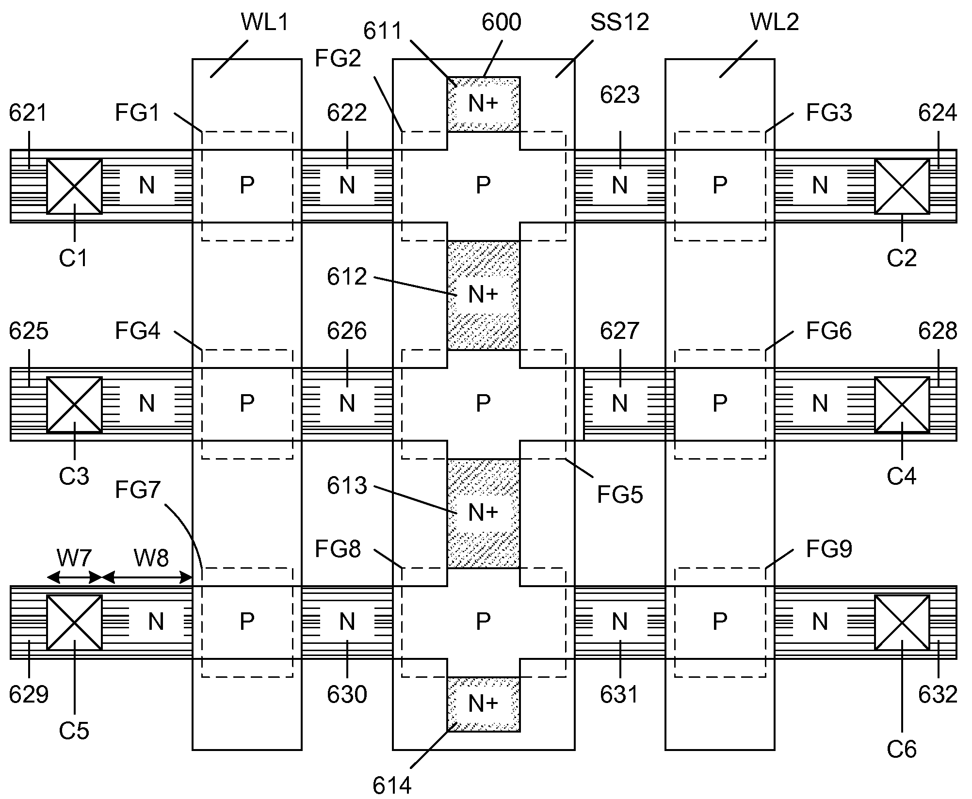
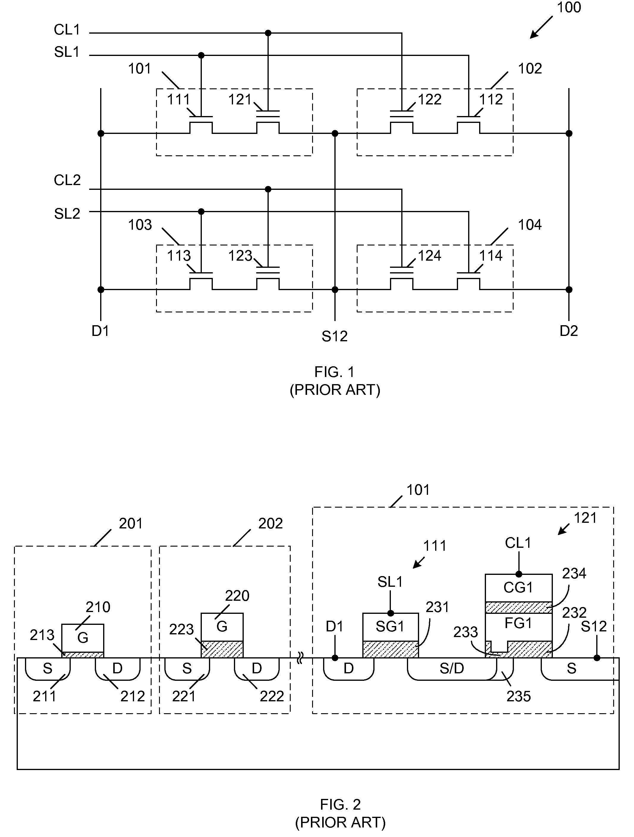
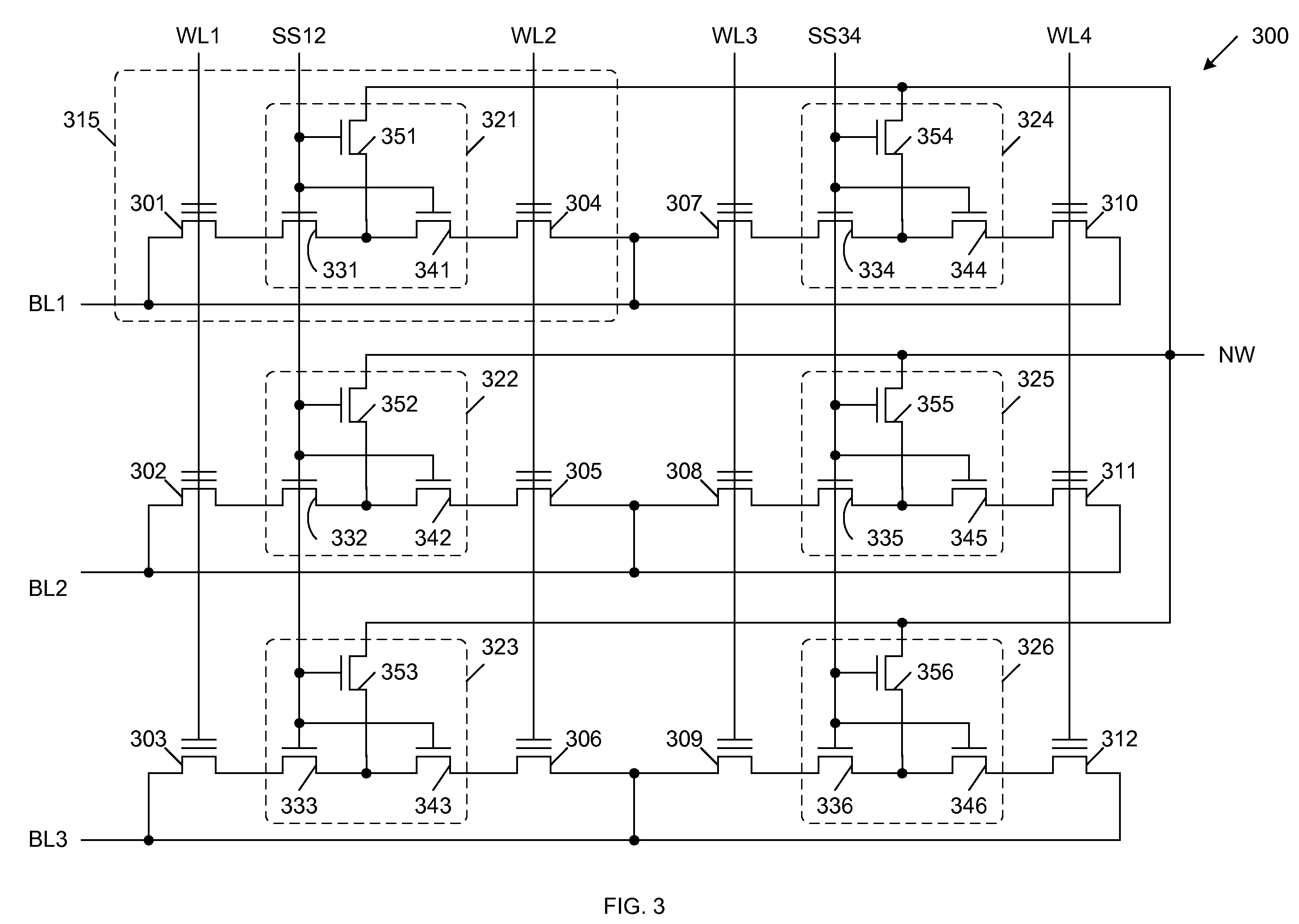
[0019]FIG. 3 is a circuit diagram of an array 300 of EEPROM cells in accordance with one embodiment of the present invention. EEPROM cell array 300 includes floating gate non-volatile memory transistors 301-312, source access transistors 321-326, word lines WL1-WL4, bit lines BL1-BL3, source select lines SS12 and SS34 and N-well connection NW. Source access transistors 321-326 include transistor structures 331-336, respectively, transistor structures 341-346, respectively, and transistor structures 351-356, respectively. As described in more detail below, each of source access transistors 321-326 implements the functionality of three transistor structures using a single transistor.

[0020]Memory transistors 301-312 and source access transistors 321-326 are fabricated in a well region having a first conductivity type, which in turn, is located in a well region having a second conductivity type, opposite the first conductivity type. In the described embodiments, memory transistors 301-3...


PUM


Abstract

A non-volatile memory including one or more EEPROM cell pairs. Each EEPROM cell pair includes three transistors and stores two data bits, effectively providing a 1.5 transistor EEPROM cell. An EEPROM cell pair includes a first non-volatile memory transistor, a second non-volatile memory transistor and a source access transistor. The source access transistor includes: a first source region continuous with a source region of the first non-volatile memory transistor; a second source region continuous with a source region of the second non-volatile memory transistor, and a drain region that extends downward through a first well region to contact a second well region. The first, second and third semiconductor regions and the second well region have a first conductivity type, and the first well region has a second conductivity type, opposite the first conductivity type.

Description

FIELD OF THE INVENTION[0001]The present invention relates to electrically erasable and programmable memory (EEPROM) cells.RELATED ART[0002]FIG. 1 is a circuit diagram illustrating a conventional memory system 100 that includes a 2×2 array of electrically erasable and programmable memory (EEPROM) cells 101-104. EEPROM cells 101-104 include CMOS access transistors 111-114, respectively, and non-volatile memory (NVM) transistors 121-124, respectively. The drains of access transistors 111 and 113 are coupled to drain (bit line) terminal D1. Similarly, the drains of access transistors 112 and 114 are coupled to drain (bit line) terminal D2. The sources of access transistors 111-114 are coupled to the drains of NVM transistors 121-124, respectively. The sources of NVM transistors 121-124 are commonly coupled to source terminal S12. The select gates of access transistors 111-112 are commonly connected to select line SL1, and the select gates of access transistors 113-114 are commonly conne...

Claims


Application Information

Patent Timeline
Patent Type & Authority Patents(United States)
IPC IPC(8): H01L29/76
CPCG11C16/0433H01L27/105H01L27/11526H01L27/11529H10B41/41H10B41/40H10B63/80
Inventor GEORGESCU, SORIN S.COSMIN, ADAM PETERSMARANDOIU, GEORGE
Owner SEMICON COMPONENTS IND LLC
Why Eureka
Try Eureka