Force sensor chip

a technology of force sensor and sensor chip, which is applied in the direction of force/torque/work measurement apparatus, instruments, and measurement of tension, etc., can solve the problems of considerable limitation in design freedom of disclosed six-axis force sensors, and the inability to ignore inter-axis interference problems, so as to achieve significant enhancement of the design freedom of the sensor chip and the ability to prevent the concentration of stress

Active Publication Date: 2009-05-26
HONDA MOTOR CO LTD
View PDF3 Cites 17 Cited by
  • Summary
  • Abstract
  • Description
  • Claims
  • Application Information

AI Technical Summary

Benefits of technology

[0010]In view of the foregoing prior art problems, it is an object of the present invention to provide an improved force sensor chip which allows an external force to be applied thereto in a dispersed manner so that stress occurring due to bending or twisting of a substrate of the chip can be dispersed, and which can have an enhanced design freedom.
[0012]Namely, the force sensor chip of the present invention includes the plurality of operating parts so that an external force input from the outside is applied to the individual operating parts in a dispersed manner. As a result, stress generated in response to bending or twisting of a base member (e.g., semiconductor substrate) of the force sensor chip can be dispersed, so that concentration of stress can be reliably prevented. Further, the construction (number, positions, shapes, etc.) of the operating parts can be modified as desired by modifying the number, positions, shapes, etc. of holes formed in the base member, with the result that design freedom of the sensor chip can be significantly enhanced.

Problems solved by technology

Generally, in the field of multi-axis force sensors, there would be encountered the problem of interference from other axes (i.e., inter-axis interference problem) that prevents individual components (i.e., forces and moments) of an external force, applied to the strain-generating body, from being accurately separated from one another or resolved with good precision.
The inter-axis interference problem can not be ignored when putting a multi-axis force sensor to practical use.
If the operating part has a relatively large area, on the other hand, load bearing performance can be enhanced; however, there is a tradeoff between the enhanced load bearing performance and miniaturization of the operating part.
As a consequence, the disclosed six-axis force sensors are considerably limited in design freedom depending on a state of stress occurring in the operating part.

Method used


Image

  • Force sensor chip
  • Force sensor chip
  • Force sensor chip

Examples


Embodiment Construction

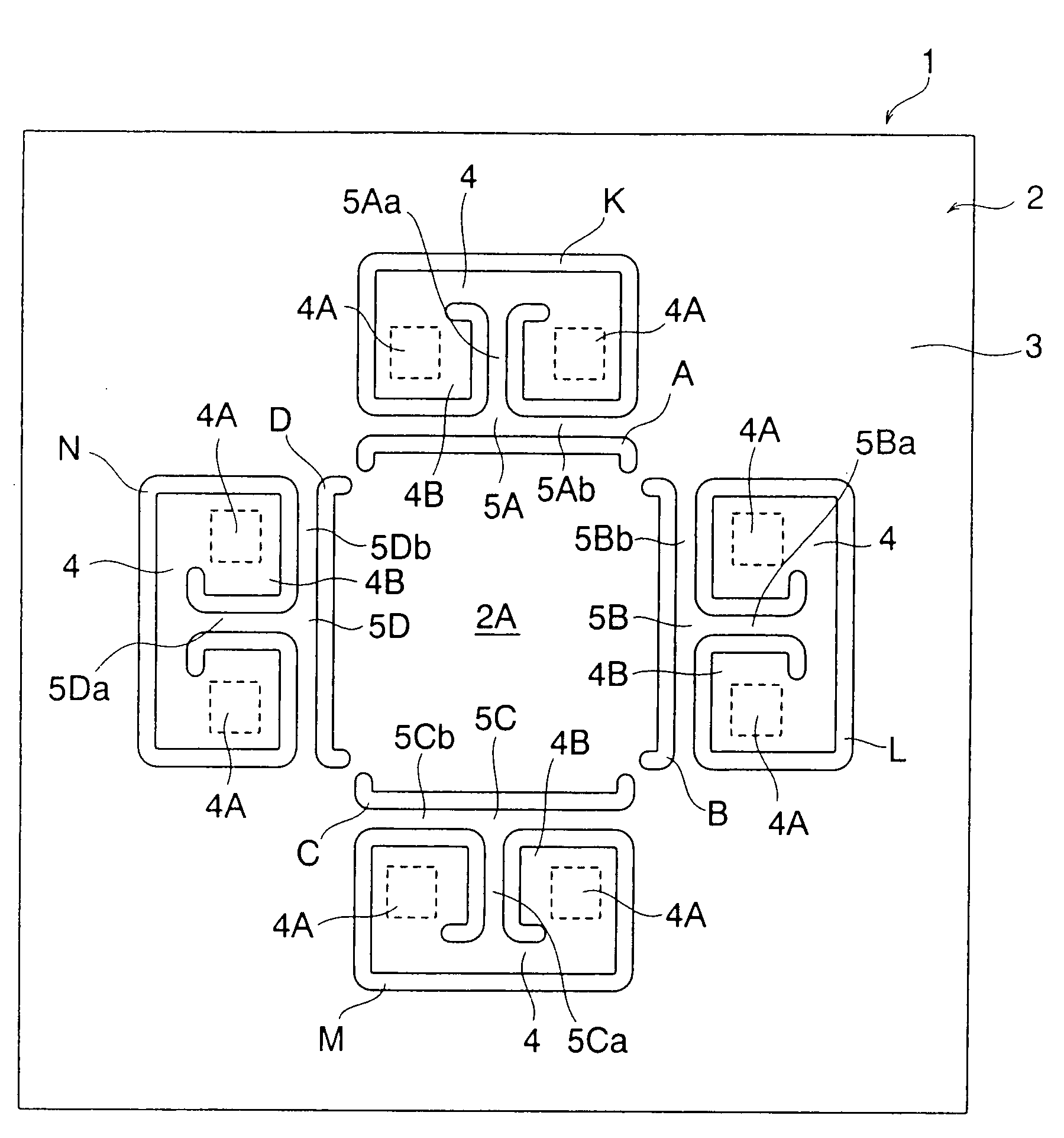
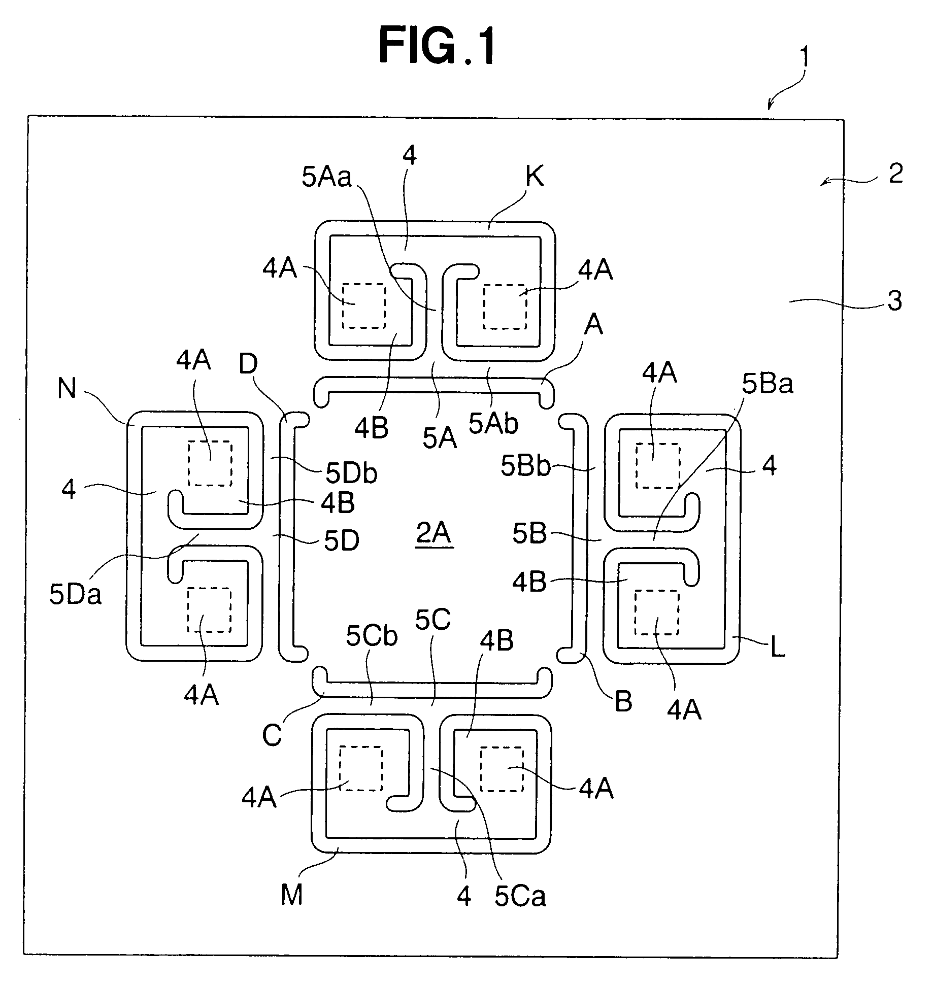
[0030]Now, with reference to FIGS. 1-10, a description will be given about a force sensor chip in accordance with a first embodiment of the present invention. The instant embodiment of the force sensor chip will be described hereinbelow as being in the form of a six-axis force sensor chip, although the present invention is not limited to a six-axis force sensor chip.

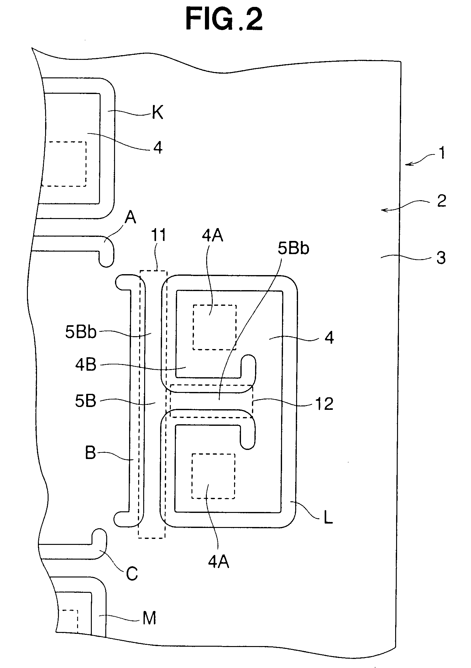
[0031]FIG. 1 is a plan view showing one surface (i.e., front surface) of the force sensor chip 1, and FIG. 2 shows in enlarged scale characteristic sections in FIG. 1. In FIGS. 1 and 2, there is only shown a planer shape of a base member (in this case, semiconductor substrate) 2 with illustration of strain resistance elements and wiring patterns omitted. FIG. 3 shows twelve strain resistance elements and some of electric wiring patterns and electrode pads provided on the semiconductor substrate 2 of the force sensor chip. FIG. 4 is a view, similar to FIG. 2, which shows in enlarged scale principal or relevant sections of...


PUM


Abstract

In a force sensor chip, a semiconductor substrate includes: a plurality of operating parts each including an external-force acting area section and a non-deforming section; a supporting part for supporting the operating parts, and a plurality of connecting parts for connecting the operating parts and the supporting part. Strain resistance elements are provided on deformation-generating sections of the connecting parts. The plurality of operating parts are provided, in corresponding relation to the plurality of connecting parts, between the connecting parts and the supporting part.

Description

FIELD OF THE INVENTION[0001]The present invention relates generally to force sensor chips, and more particularly to an improved force sensor chip which has a plurality of strain resistance elements formed on a substrate using semiconductor manufacturing technology and which is suitable for use a six-axis force sensor or other device in an industrial robot or the like.BACKGROUND OF THE INVENTION[0002]As known in the art, automated working machines, such as machine tools and industrial robots, apply forces to workpieces and are themselves subjected to external forces because of the manner in which these machines operate. In this case, it is necessary for the working machines to detect external forces and moments applied to the machines and to perform control corresponding to the detected external forces and moments. In order to perform the control, corresponding to the detected external forces and moments, with a high degree of precision, it is required to accurately detect the extern...

Claims


Application Information

Patent Timeline
Patent Type & Authority Patents(United States)
IPC IPC(8): G01D7/00
CPCG01L1/205
Inventor SAKURAI, NOBUHIROOHSATO, TAKESHI
Owner HONDA MOTOR CO LTD
Why Eureka
Try Eureka