Capacitive micro-electro-mechanical sensors with single crystal silicon electrodes

a micro-electromechanical and sensor technology, applied in the field of sensors, can solve the problems of thermal mismatch between the top and bottom of the gap, reduce the accuracy and durability of capacitive sensors, and limit the ability to seal the device hermetically

Active Publication Date: 2009-05-26
SAMSUNG ELECTRONICS CO LTD
View PDF14 Cites 64 Cited by
  • Summary
  • Abstract
  • Description
  • Claims
  • Application Information

AI Technical Summary

Benefits of technology

[0007]In another preferred embodiment, the sensor further includes a third single crystal silicon layer, which is separated from the top surface of the top layer by a dielectric layer. In one embodiment, this third layer is etched to define a pressure port. In this embodiment, the sensor senses pressure, with the advantage that the pressure port is on the opposite side of the device from the electrical contacts.

Problems solved by technology

Several fabrication features cause a reduction in the accuracy and durability of capacitive sensors.
The use of different materials on the top and bottom surfaces of the capacitive gap leads to thermal mismatch between the top and bottom of the gap.
Use of metal electrodes limits the ability to form a high temperature fusion bond between two wafers, which limits the ability to seal the device hermetically.
Construction of a pressure port on the same surface as the wirebond pads leads to a difficult exposure problem of the wirebond pads to the harsh media being measured.
However, these fabrication methods have several disadvantages.
In addition, the use of metal gives rise to the complications described above.

Method used


Image

  • Capacitive micro-electro-mechanical sensors with single crystal silicon electrodes
  • Capacitive micro-electro-mechanical sensors with single crystal silicon electrodes
  • Capacitive micro-electro-mechanical sensors with single crystal silicon electrodes

Examples


Embodiment Construction

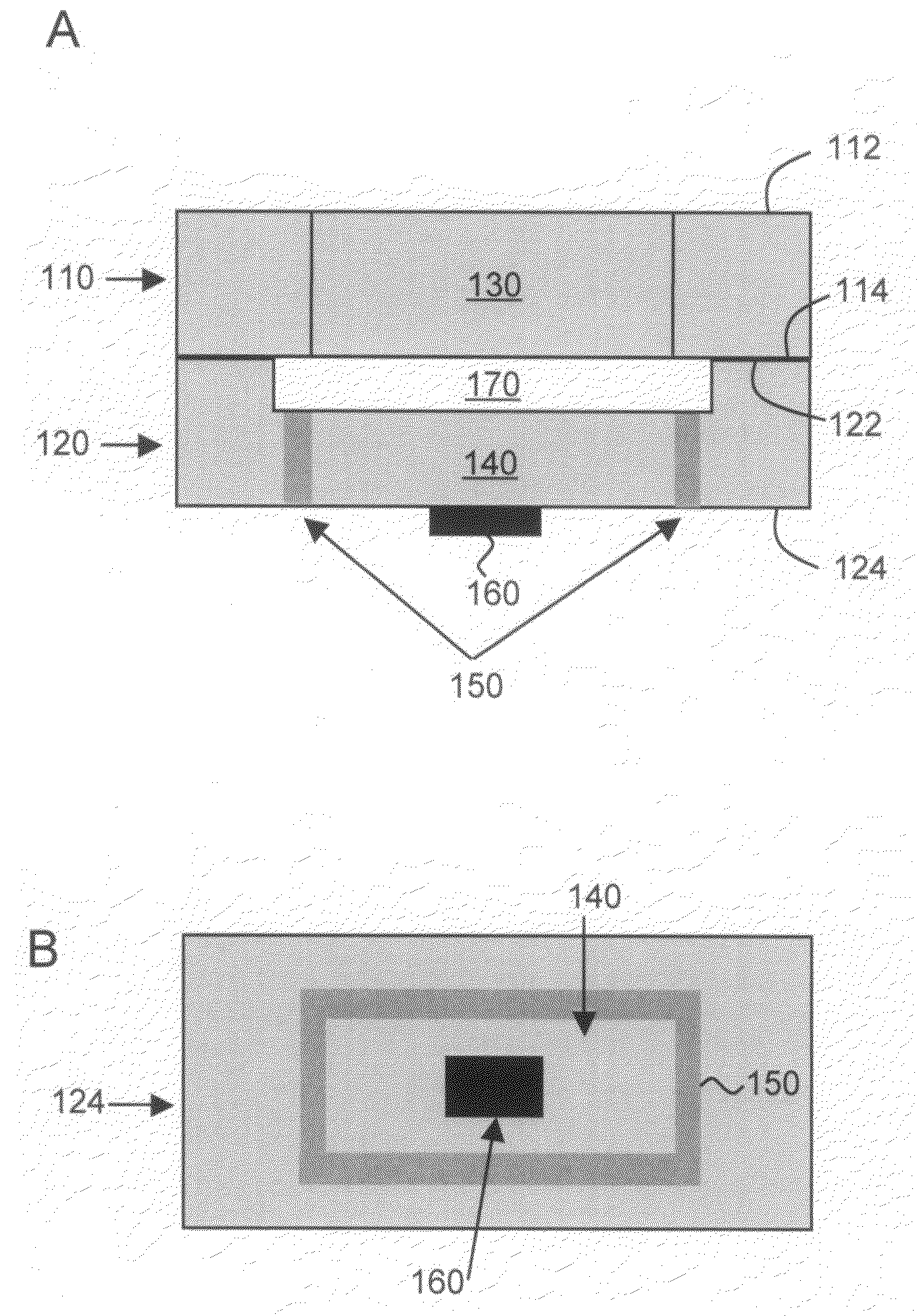
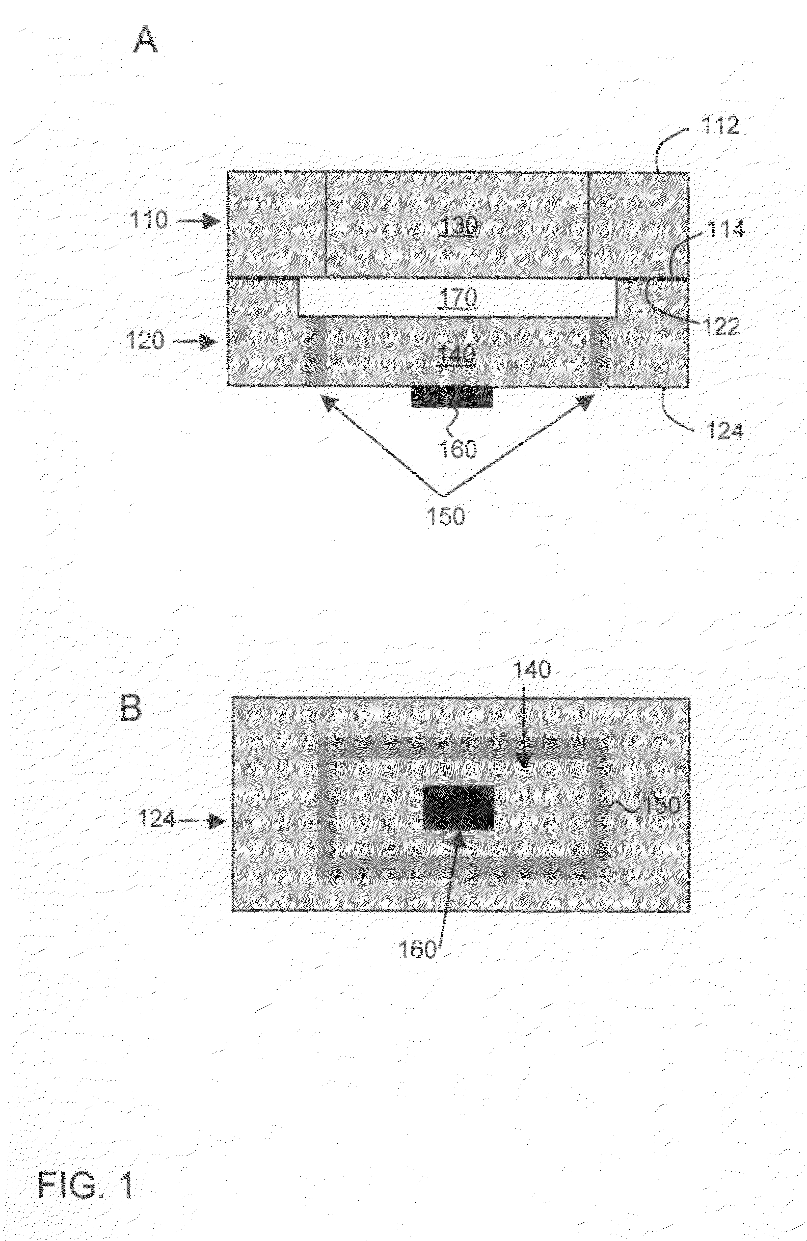
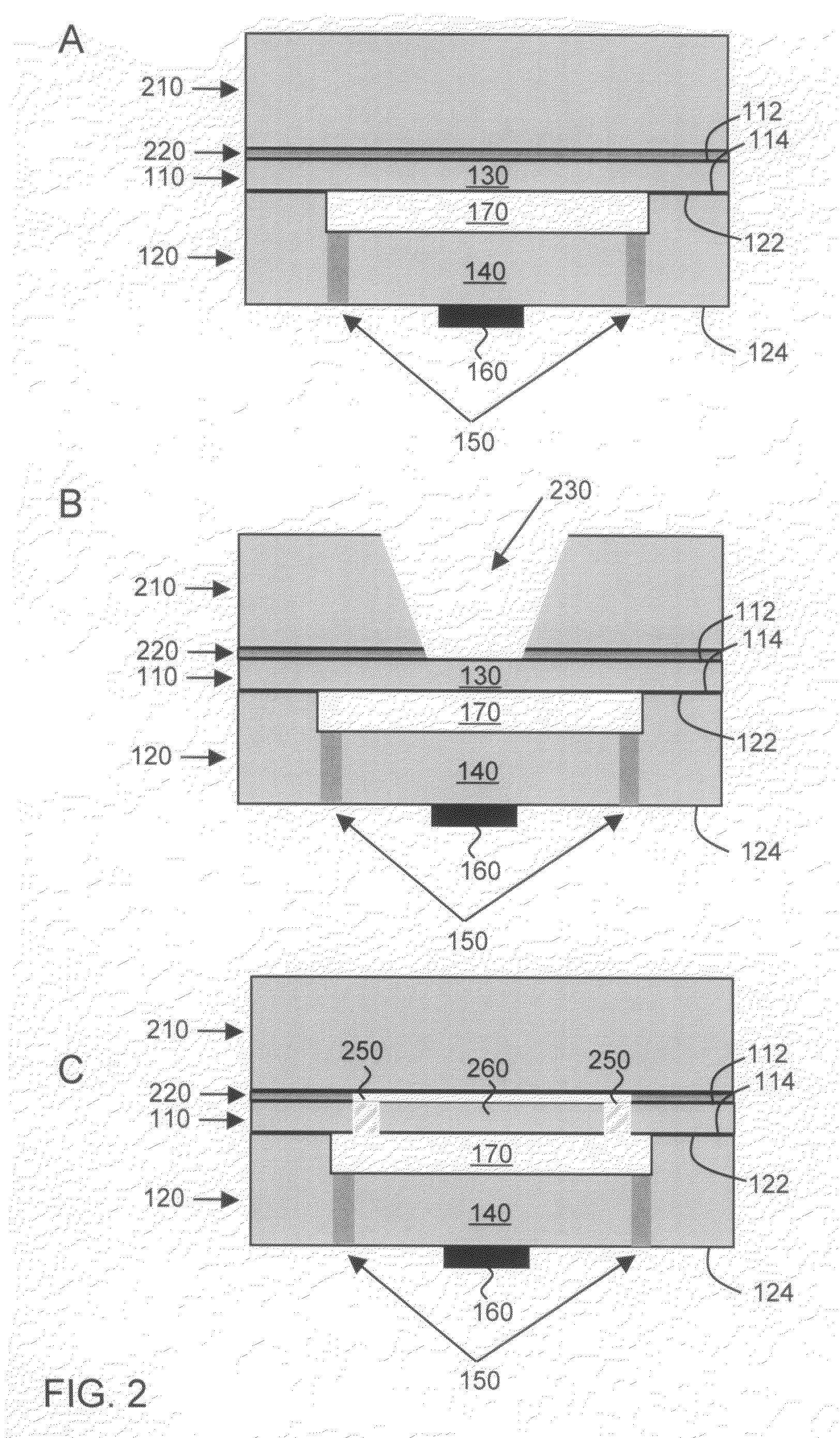
[0015]In the following description, structures that appear in different figures are identically labeled.

[0016]FIG. 1A shows a cross-sectional view of a capacitive micro-electromechanical sensor according to the present invention. The sensor includes a first layer 110, with top surface 112 and bottom surface 114. First layer 110 is made of single crystal silicon and contains at least one electrode 130. The sensor further includes a second layer 120, with a top surface 122 and a bottom surface 124. Second layer 120 contains an isolating trench 150 made of dielectrical material that extends from top surface 122 to bottom surface 124. Isolating trench 150 defines electrode 140. Electrode 140 is electrically connected to electrical contact 160, such as a wire-bond pad. Preferably, first layer 110 contains all of the sensing elements of the sensor, such that the sensing elements are on the opposite side of the sensor to electrical contact 160. Electrodes 130 and 140 together define a capa...


PUM


Abstract

The devices presented herein are capacitive sensors with single crystal silicon on all key stress points. Isolating trenches are formed by trench and refill forming dielectrically isolated conductive silicon electrodes for drive, sense and guards. For pressure sensing devices according to the invention, the pressure port is opposed to the electrical wire bond pads for ease of packaging. Dual-axis accelerometers measuring in plane acceleration and out of plane acceleration are also described. A third axis in plane is easy to achieve by duplicating and rotating the accelerometer 90 degrees about its out of plane axis Creating resonant structures, angular rate sensors, bolometers, and many other structures are possible with this process technology. Key advantages are hermeticity, vertical vias, vertical and horizontal gap capability, single crystal materials, wafer level packaging, small size, high performance and low cost.

Description

CROSS-REFERENCE TO RELATED APPLICATIONS[0001]This application claims priority from U.S. Provisional Patent Application No. 60 / 791,790, filed Apr. 13, 2006, which is incorporated herein by reference. This application is a continuation-in-part of U.S. patent application Ser. No. 11 / 292,946, filed Dec. 1, 2005, which is incorporated herein by reference.FIELD OF THE INVENTION[0002]The present invention relates generally to sensors. More particularly, the present invention relates to capacitive micro-electro-mechanical sensors with single crystal silicon electrodes.BACKGROUND[0003]Several fabrication features cause a reduction in the accuracy and durability of capacitive sensors. The use of different materials on the top and bottom surfaces of the capacitive gap leads to thermal mismatch between the top and bottom of the gap. Use of metal electrodes limits the ability to form a high temperature fusion bond between two wafers, which limits the ability to seal the device hermetically. Cons...

Claims


Application Information

Patent Timeline
Patent Type & Authority Patents(United States)
IPC IPC(8): H01G7/00G01C19/56G01C19/5769
CPCB81B3/0021G01L9/0073G01P15/0802G01P15/125G01P15/18B81B2201/0235B81B2201/0242B81B2201/0264H01L28/40G01P2015/0814G01P2015/0831G01P2015/084
Inventor RAY, CURTIS A.BRYZEK, JANUSZ
Owner SAMSUNG ELECTRONICS CO LTD
Why Eureka
Try Eureka