Silicon oxide thin-films with embedded nanocrystalline silicon
What is AI technical title?
AI technical title is built by PatSnap AI team. It summarizes the technical point description of the patent document.
a technology of nanocrystalline silicon and silicon oxide, which is applied in the direction of coating, chemical vapor deposition coating, coating process, etc., can solve the problems of low plasma density, low ion/neutral ratio, low plasma density, and inefficient power coupling to the plasma, so as to minimize the plasma induced bulk and interface damage, the effect of improving the kinetics of plasma reaction
Inactive Publication Date: 2009-06-09
SHARP KK
View PDF4 Cites 11 Cited by
Summary
Abstract
Description
Claims
Application Information
AI Technical Summary
This helps you quickly interpret patents by identifying the three key elements:
Problems solved by technology
Method used
Benefits of technology
Benefits of technology
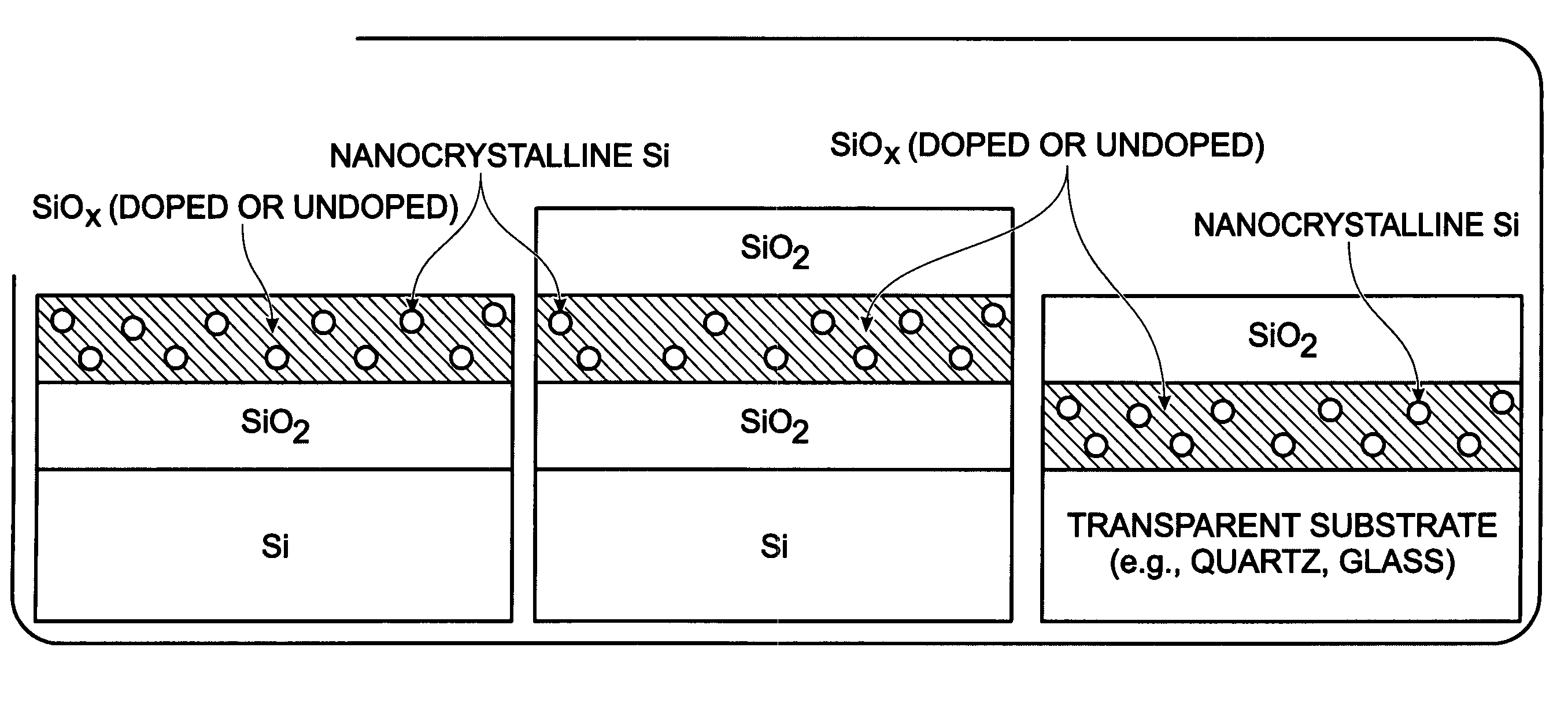
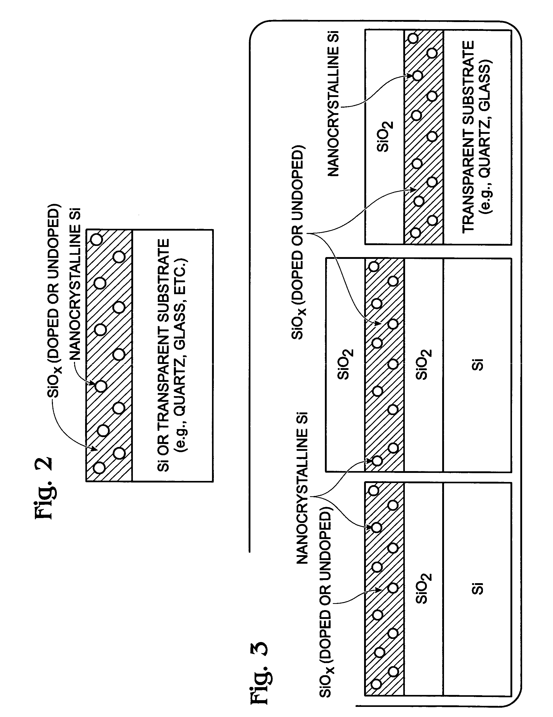
[0018]This invention describes a novel high-density plasma-based processes for the fabrication of nanocrystalline Si-embedded SiOx thin films with controlled microstructural, optical, and electrical properties. The high-density plasma technique is characterized by high plasma concentrations, low plasma potential, and independent control of plasma energy and density, which provide unique process possibilities and control. The high-density plasma characteristics are suitable for novel thin-film fabrication due to enhanced plasma reaction kinetics. The high-density plasma deposition process is dominantly controlled by the plasma characteristics rather than the thermal state of the substrate. The high plasma density and low plasma potential of the high-density plasma process are attractive for the creation of the Si nanocrystals, while minimizing the plasma induced bulk and interface damage.
[0021]The SiOx thin-film with embedded nanocrystalline Si typically has a refractive index in the range of about 1.6 to 2.2. The refractive index of the SiOx thin-film can be increased in response to increasing the ratio of hydrogen to silicon precursor. If the oxygen source gas and silicon precursor are mixed with a noble gas, where the ratio of noble gas to silicon precursor in the range of about 0.02 to 10, then the refractive index of the SiOx thin film can be increased in response to increasing the ratio of noble gas to silicon precursor. The refractive index of the SiOx thin-film can also be increased by decreasing the RF power to the top electrode, or by increasing the ratio of silicon precursor to oxygen source gas.
Problems solved by technology
However, the indirect band-gap makes it an inefficient material for optoelectronic devices.
However, conventional PECVD and sputtering techniques have the limitations of low plasma density, inefficient power coupling to the plasma, low ion / neutral ratio, and uncontrolled bulk, and interface damage due to high ion bombardment energy.
Therefore, the oxide films formed from a conventional capacitively-coupled plasma (CCP) generated plasma may create reliability issues due to the high bombardment energy of the impinging ionic species.
However, it is not possible to control the ion energy using radio frequency (RF) of CCP generated plasma.
Any attempt to enhance the reaction kinetics by increasing the applied power results in increased bombardment of the deposited film, which creates a poor quality films with a high defect concentration.
Additionally, the low plasma density associated with these types of sources (˜1×10⁸-109 cm−3) leads to limited reaction possibilities in the plasma and on the film surface, inefficient generation of active radicals for enhanced process kinetics, inefficient oxidation, and reduction of impurities at low thermal budgets, which limits their usefulness in the fabrication of low-temperature electronic devices.
The higher temperature thermal processes can interfere with the other device layers and it is not suitable in terms of efficiency and thermal budget, due to the lower reactivity of the thermally activated species.
It may not be possible to learn or develop thin-films by just extending the processes developed in low density plasma or other high density plasma systems, as the plasma energy, composition (radical to ions), plasma potential, electron temperature, and thermal conditions correlate differently depending on the process map.
Method used
Image
Click on the blue label to locate the original text in one second.
Reading with bidirectional positioning of images and text.
Examples
Embodiment Construction
High-Density Plasma System
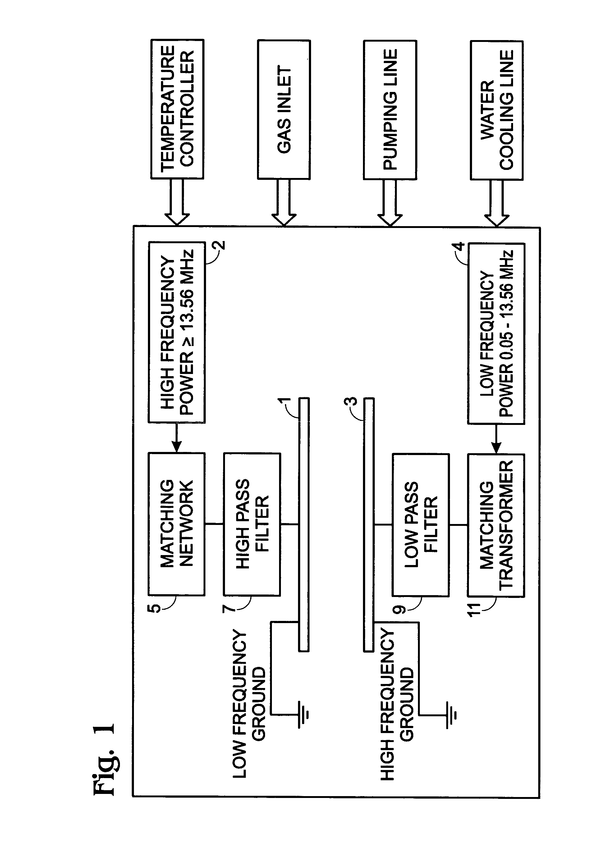
[0031]FIG. 1 is a schematic drawing of a high-density plasma (HDP) system with an inductively coupled plasma source. The top electrode 1 is driven by a high frequency radio frequency (RF) source 2, while the bottom electrode 3 is driven by a lower frequency power source 4. The RF power is coupled to the top electrode 1, from the high-density inductively coupled plasma (ICP) source 2, through a matching network 5 and high pass filter 7. The power to the bottom electrode 3, through a low pass filter 9 and matching transformer 11, can be varied independently of the top electrode 1. The top electrode power frequency can be in the range of about 13.56 to about 300 megahertz (MHz) depending on the ICP design. The bottom electrode power frequency can be varied in the range of about 50 kilohertz (KHz) to about 13.56 MHz, to control the ion energy. The pressure can be varied up to 500 mTorr. The top electrode power can be as great as about 10 watts per square-centim...
PUM
Property
Measurement
Unit
frequency
aaaaa
aaaaa
pressure
aaaaa
aaaaa
temperature
aaaaa
aaaaa
Abstract
A method is provided for forming a silicon oxide (SiOx) thin-film with embedded nanocrystalline silicon (Si). The method deposits SiOx, where x is in the range of 1 to 2, overlying a substrate, using a high-density (HD) plasma-enhanced chemical vapor deposition (PECVD) process. As a result, the SiOx thin-film is embedded with nanocrystalline Si. The HD PECVD process may use an inductively coupled plasma (ICP) source, a substrate temperature of less than about 400° C., and an oxygen source gas with a silicon precursor. In one aspect, a hydrogen source gas and an inert gas are used, where the ratio of oxygen source gas to inert gas is in the range of about 0.02 to 5. The SiOx thin-film with embedded nanocrystalline Si typically has a refractive index in the range of about 1.6 to 2.2, with an extinction coefficient in the range of 0 to 0.5.
Description
RELATED APPLICATIONS[0001]This application is a continuation-in-part of a pending patent application entitled, ENHANCED THIN-FILM OXIDATION PROCESS, invented by Pooran Joshi et al., Ser. No. 11 / 327,612, filed Jan. 6, 2006.[0002]This application is a continuation-in-part of a pending patent application entitled, HIGH-DENSITY PLASMA HYDROGENATION, invented by Pooran Joshi et al., Ser. No. 11 / 013,605, filed Dec. 15, 2004.[0003]This application is a continuation-in-part of a pending patent application entitled, DEPOSITION OXIDE WITH IMPROVED OXYGEN BONDING, invented by Pooran Joshi, Ser. No. 10 / 801,377, filed Mar. 15, 2004 now U.S. Pat. No. 7,122,487.[0004]This application is a continuation-in-part of a pending patent application entitled, HIGH-DENSITY PLASMA OXIDATION FOR ENHANCED GATE OXIDE PERFORMANCE, invented by Joshi et al., Ser. No. 11 / 139,726, filed May 26, 2005 now U.S. Pat. No. 7,381,595.[0005]This application is a continuation-in-part of a pending patent application entitled,...
Claims
Application Information
Patent Timeline
Application Date:The date an application was filed.
Publication Date:The date a patent or application was officially published.
First Publication Date:The earliest publication date of a patent with the same application number.
Issue Date:Publication date of the patent grant document.
PCT Entry Date:The Entry date of PCT National Phase.
Estimated Expiry Date:The statutory expiry date of a patent right according to the Patent Law, and it is the longest term of protection that the patent right can achieve without the termination of the patent right due to other reasons(Term extension factor has been taken into account ).
Invalid Date:Actual expiry date is based on effective date or publication date of legal transaction data of invalid patent.

