Method of forming light-emitting element

a technology of light-emitting elements and substrates, which is applied in the direction of discharge tubes/lamp details, thermoelectric devices, discharge tubes luminescnet screens, etc., can solve the problems of reducing affecting the efficiency of recycling, so as to suppress the deterioration of substrates and reduce the cost

Inactive Publication Date: 2009-06-23
CANON KK
View PDF8 Cites 28 Cited by
  • Summary
  • Abstract
  • Description
  • Claims
  • Application Information

AI Technical Summary

Benefits of technology

[0011]For this reason, an object of the present invention is to provide a method of forming a light-emitting element at a lower cost than a conventional cost, while suppressing the deterioration of the substrate due to thermal distortion in comparison with a conventional method of recycling a substrate and further having an effect equal to that of the conventional method of recycling a substrate.
[0014]The method of forming a light-emitting element according to the present invention provides an effect of recycling a substrate while keeping a lower cost and a lower stress of the substrate (leading to higher crystalline quality) than a normal method of transferring a film and recycling a substrate.

Problems solved by technology

Accordingly, when the substrates having a size of a substrate scale (normally, 2 inches Φ or larger) are separated from each other, it takes an extremely long period of time to separate the substrates by a method of etching the separation layer mainly from side faces of the substrates.
In actual fact, however, the technology has a disadvantage that when the films are repeatedly grown thereon at a high temperature, the substrate becomes very brittle because distortion is accumulated in the substrate due to heat, and has been technically difficult.
In addition, the technology has lost one half its initial effectiveness of recycling because a cost of epitaxial growth is high as well as a substrate cost.

Method used


Image

  • Method of forming light-emitting element
  • Method of forming light-emitting element
  • Method of forming light-emitting element

Examples


first example

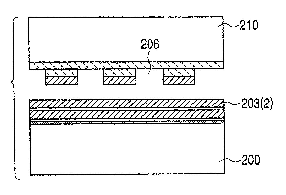
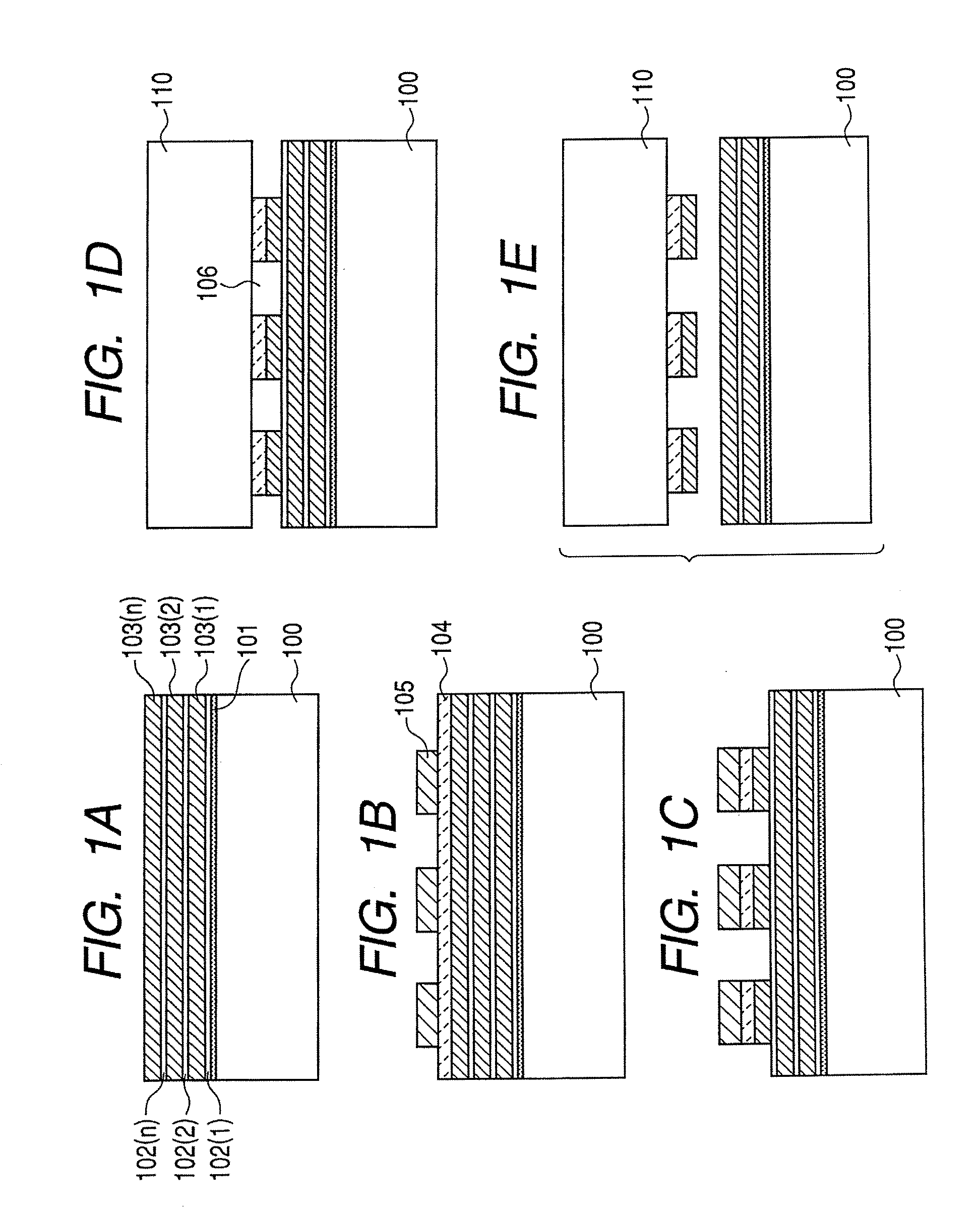
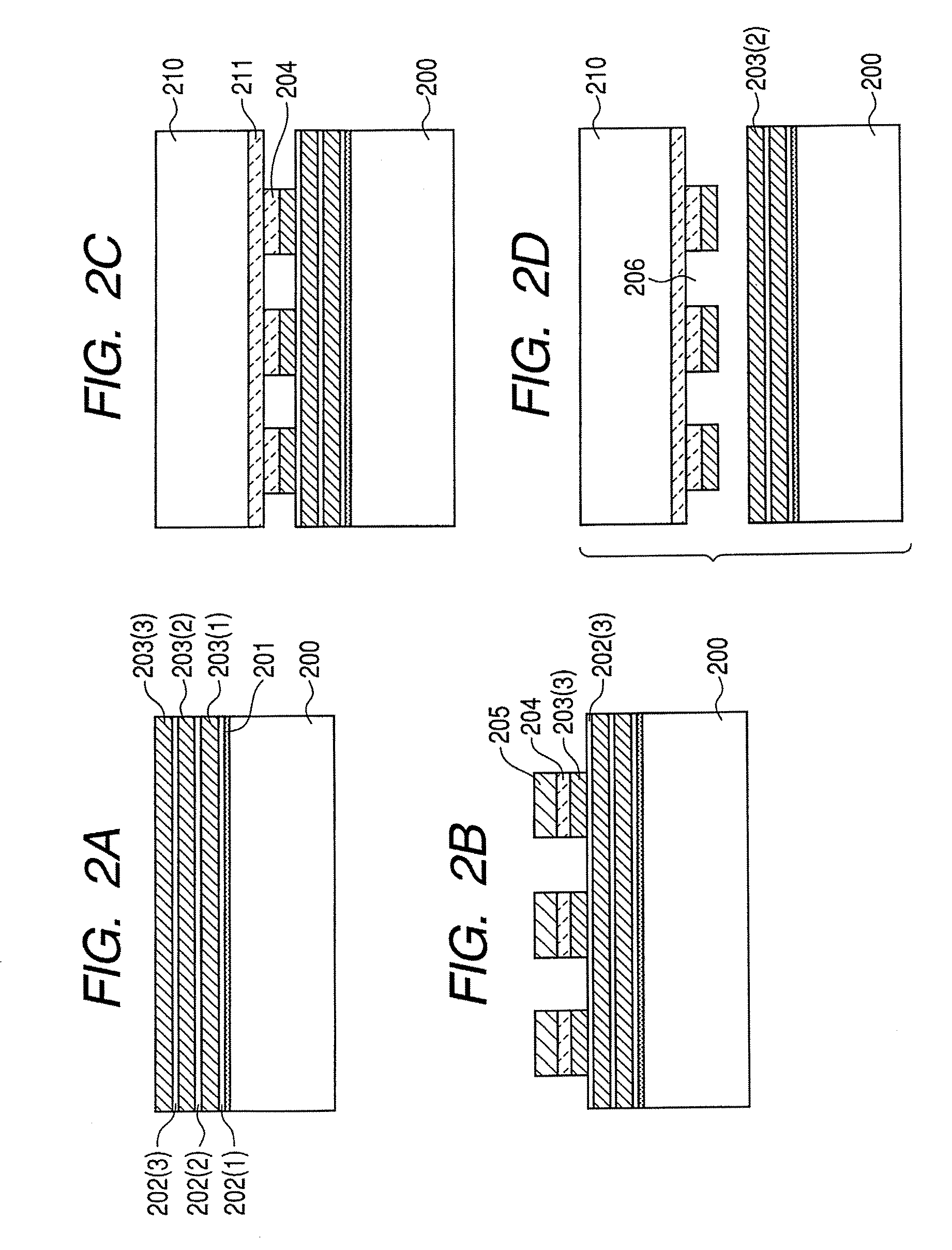
[0051]A first example according to the present invention will be now described with reference to FIGS. 2A to 2D. In the figures, reference numeral 200 denotes the first substrate, reference numeral 201 denotes a buffer layer, reference numeral 202 denotes a separation layer, reference numeral 203 denotes an active layer (light-emitting layer), reference numeral 204 denotes a light reflection layer, reference numeral 205 denotes a resist film, reference numeral 206 denotes an etched groove, and reference numeral 210 denotes the second substrate.

[0052]At first, a GaAs buffer layer 201 with a thickness of 20 nm, a p-AlAs layer 202(1) with a thickness of 100 nm, and an active layer 203(1) with a thickness of about 2,000 nm are grown on a 4-inch GaAs substrate 200 by an MOCVD method, as is illustrated in FIG. 2A.

[0053]The active layer 203(1) will be now described in detail below.

[0054]Specifically, the active layer 203(1) includes a p-GaAs layer to be a contact layer with the thickness o...

second example

[0067]A second example according to the present invention will be now described with reference to FIGS. 3A and 3B.

[0068]The same substrate as in the first example is prepared, an Au film is formed thereon, and the pattern is formed in the same manner as in the first example. However, an island-shaped region to be patterned is a rectangular shape having an area of 8 mm×0.5 mm.

[0069]Afterwards, the light-emitting element region of 8 mm×0.5 mm is transferred onto a silicon substrate in the same process to that in the first example.

[0070]The silicon substrate is charged into an LED process, and is produced into elements with the size of 20×20 μm arrayed at spacings of 600 dpi in the process.

third example

[0071]In the present example, the same steps as in the first example are carried out, but the following items are changed.

[0072]A Ge (germanium) substrate with the size of 8 inches is used as the first substrate. A silicon substrate with the size of 8 inches is used as the second substrate. A light reflection layer is not formed on a silicon substrate.

[0073]The present invention can be used in a method of forming a light-emitting element, and a method of forming a light-emitting element particularly by separating an active layer at a separation layer to form an active layer on a substrate.


PUM


Abstract

An object of the present invention is to provide a method of forming a light-emitting element at a lower cost than a conventional cost with suppressing the deterioration of the substrate due to thermal distortion in comparison with a conventional method of recycling a substrate and further having an effect equal to that of the method of recycling a substrate. The method of forming a light-emitting element by growing a separation layer and a light-emitting layer in this order on a first substrate, bonding the light-emitting layer onto a second substrate, and removing the separation layer to form the light-emitting layer on the second substrate, includes growing a plurality of groups each containing the separation layer and light-emitting layer on the first substrate; patterning the light-emitting layer existing as a uppermost layer into an island shape, and then bonding the light-emitting layer onto the second substrate, and etching the separation layer adjacent to the light-emitting layer patterned into the island shape to form the light-emitting layer patterned into the island shape on the second substrate.

Description

BACKGROUND OF THE INVENTION[0001]1. Field of the Invention[0002]The present invention relates to a method of forming a light-emitting element, specifically a method of forming a light-emitting element by separating an active layer at a separation layer to form the active layer on a substrate.[0003]2. Description of the Related Art[0004]Some technologies for transferring an active layer onto a supporting substrate by bonding a substrate having a separation layer and an active layer onto the supporting substrate and then separating the bonded substrate at the separation layer have been disclosed by, for example, Japanese Patent Application Laid-Open No. 2004-146537.[0005]In the above described technologies, however, the bonded substrates are separated by etching the separation layer. Accordingly, when the substrates having a size of a substrate scale (normally, 2 inches Φ or larger) are separated from each other, it takes an extremely long period of time to separate the substrates by ...

Claims


Application Information

Patent Timeline
Patent Type & Authority Patents(United States)
IPC IPC(8): H01L21/00H01L21/30H01L21/46H01L33/08H01L33/10H01L33/30
CPCH01L33/0079H01L33/08H01L33/20H01L33/0093
Inventor YAMAGATA, KENJIYONEHARA, TAKAOSEKIGUCHI, YOSHINOBUNISHI, KOJIRO
Owner CANON KK
Why Eureka
Try Eureka