Optical device and method for producing the same

a technology of optical devices and optical connections, applied in the direction of optical elements, instruments, optical waveguide light guides, etc., can solve the problems of inconvenient mounting of optical electronic integrated circuit boards, and inability to position techniques using microlenses or right-angle bending elements, etc., to achieve excellent optical connection characteristics and less optical loss

Inactive Publication Date: 2009-06-23
BRIDGESTONE CORP
View PDF11 Cites 18 Cited by
  • Summary
  • Abstract
  • Description
  • Claims
  • Application Information

AI Technical Summary

Benefits of technology

[0009]Accordingly, an object of the present invention is to provide an optical device that has an improved optical interconnection structure between optical waveguides and optical elements to reduce connection loss and achieve excellent optical connection characteristics and also provide a method for producing the optical device.
[0010]As a result of an intensive study, the present inventors have found that optical waveguides and optical elements can be optically connected with lower loss than ever before by providing a resin layer therebetween and forming predetermined optical interconnects in the resin layer.
[0017]The present invention, as described above, can provide an optical device that causes less optical loss between an optical waveguide and an optical element than ever before and has excellent optical connection characteristics, and can also provide a method for producing the optical device.

Problems solved by technology

An important challenge for such optical devices is the reduction of connection loss between optical components.
The techniques using microlenses or right-angle bending elements, however, have difficulty in positioning them when they are mounted on an optical electronic integrated circuit board.
As a result, such techniques undesirably involve a larger number of steps for mounting.
Furthermore, foreign matter can intrude into an optical path of signal light, obstruct transmission, and cause optical loss.
The transmission of optical signals between optical waveguides and optical elements through an underfill layer for optical paths or optical signal transmission lines, as disclosed in the above publications, is unsatisfactory, and techniques for optical connection with lower loss are demanded.

Method used


Image

  • Optical device and method for producing the same
  • Optical device and method for producing the same
  • Optical device and method for producing the same

Examples


example 1

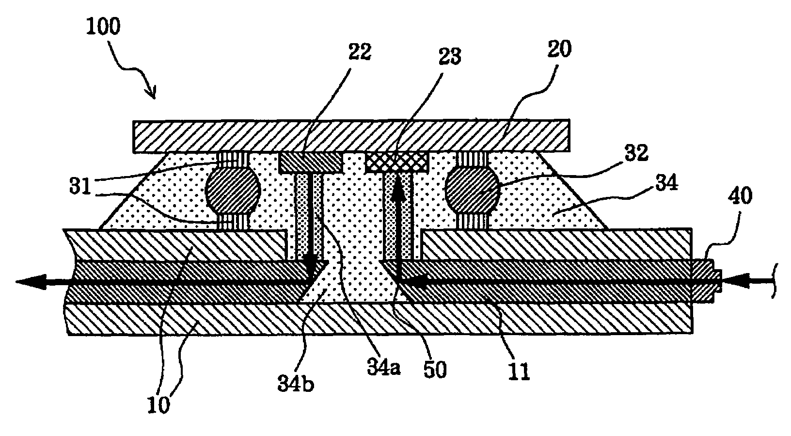
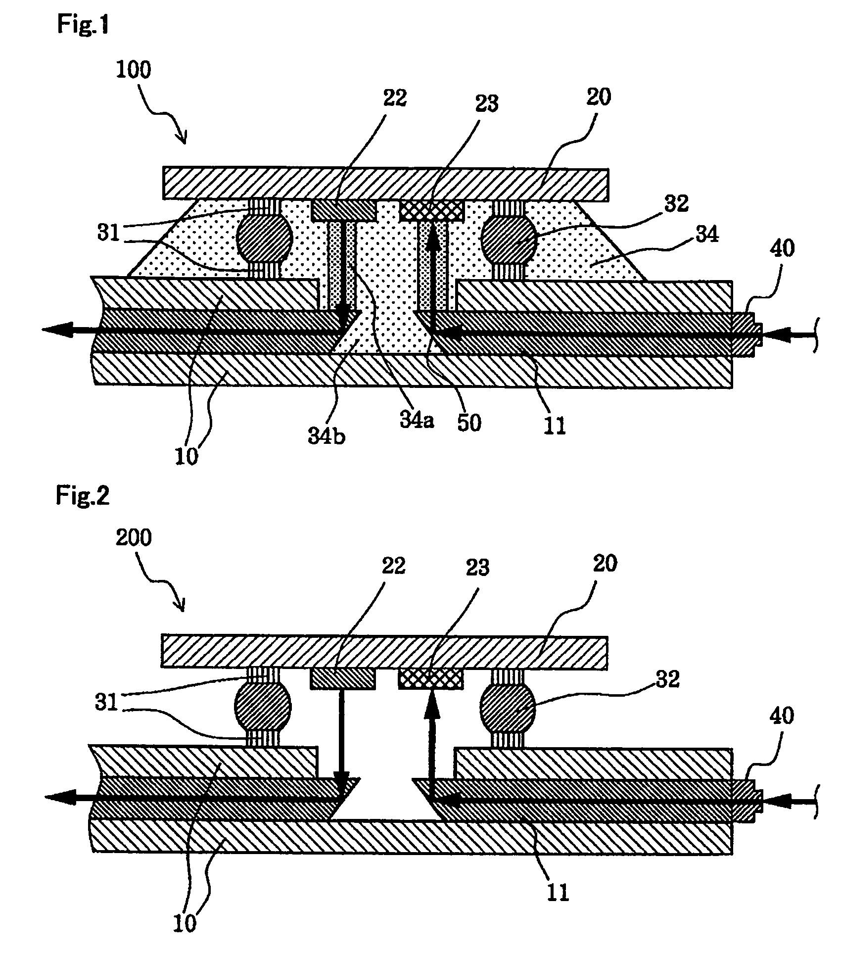
[0065]First, the 45° mirrors 50 were formed in advance by dicing at positions of the optical waveguides 11 which correspond to the optical elements (VCSEL 22 and PD 23) mounted on the IC-chip mounting substrate 20 to optically connect the optical waveguides 11 and the VCSEL 22 and PD 23. Subsequently, a printed circuit board (FR4) 10 was bonded to the optical waveguides 11 with an epoxy adhesive to prepare the printed circuit board 10, which included the optical waveguides 11 as intermediate layers. A top hole was then formed using a drill machine at a position of the printed circuit board 10 which corresponds to the optical paths between the optical waveguides 11 and the VCSEL 22 and PD 23. The printed circuit board 10, which had an electrode pattern formed in advance, was mounted on the IC-chip mounting substrate 20, which had the VCSEL 22 and PD 23, by bonding the electrodes 31 using the solder balls 32 disposed under the substrate 20. The solder balls 32 were heated using a sold...

example 2

[0069]After the VCSEL 22 and PD 23 were mounted on the printed circuit board 10 as in Example 1, the space between the 45° mirrors 50 of the optical waveguides 11 and the VCSEL 22 and PD 23 was filled using a dispenser with an epoxy underfill material prepared by mixing a photocurable material and a thermosetting material.

[0070]The underfill material was partially cured for five minutes by both light with a wavelength of 850 nm emitted from the VCSEL 22 and light with a wavelength of 850 nm that was emitted from an external laser source to reach the PD 23 through the optical waveguide 11 to form an optical waveguide structure including the optical interconnects 34a as cores (core diameter=60 μm). The overall underfill material was then heated at 150° C. for 30 minutes to cure the overall resin layer 34.

[0071]The optical interconnects 34a thus prepared exhibited an optical loss of 1.0 dB, which indicates that the optical interconnects 34a had excellent light connection characteristic...


PUM


Abstract

An optical device includes an optical waveguide, an optical element, and a resin layer disposed between the optical waveguide and the optical element. The resin layer is formed of a photocurable material alone or in combination with a thermosetting material and includes an optical interconnect for optically connecting the optical waveguide and the optical element. The optical interconnect has a higher refractive index than a region of the resin layer around the optical interconnect. A method for producing the optical device includes providing the photocurable material between the optical waveguide and the optical element, partially irradiating the photocurable material with light to form the optical interconnect, and secondarily irradiating the overall photocurable material with light to cure the overall resin layer.

Description

BACKGROUND OF THE INVENTION[0001]1. Field of the Invention[0002]The present invention relates to optical devices and methods for producing the devices, and specifically to an optical device having an improved optical interconnection structure between optical waveguides and optical elements and a method for producing the device.[0003]2. Description of the Related Art[0004]Optical interconnection technology has recently been introduced to electronic circuit boards for electronic devices to achieve higher signal transmission speeds. Specifically, an optical waveguide is stacked on an electronic circuit layer for use as an optical interconnect in a circuit board. A circuit board having both electronic and optical interconnects is generally called an optical electronic integrated circuit board.[0005]FIG. 2 shows an example of an optical electronic integrated circuit board. In FIG. 2, an optical electronic integrated circuit board 200 includes a printed circuit board 10 including optical ...

Claims


Application Information

Patent Timeline
Patent Type & Authority Patents(United States)
IPC IPC(8): G02B6/12G02B6/26G02B6/42
CPCG02B6/1221G02B6/42G02B6/4214G02B6/4239H01L2224/16225H01L2224/73204
Inventor AOKI, MASAMIMATSUSE, TAKAHIROKITANO, HIDEKI
Owner BRIDGESTONE CORP
Why Eureka
Try Eureka